---------------------------------------------------------------------------------
Design of a Network Cable Detector Based on Digital Circuits - JLCPCB EDA Open Source Hardware Platform (oshwhub.com)
Thanks to the original project shared by LCEDA, the basic principles are detailed, and replication is very simple.
---------------------------------------------------------------------------------
Purpose:
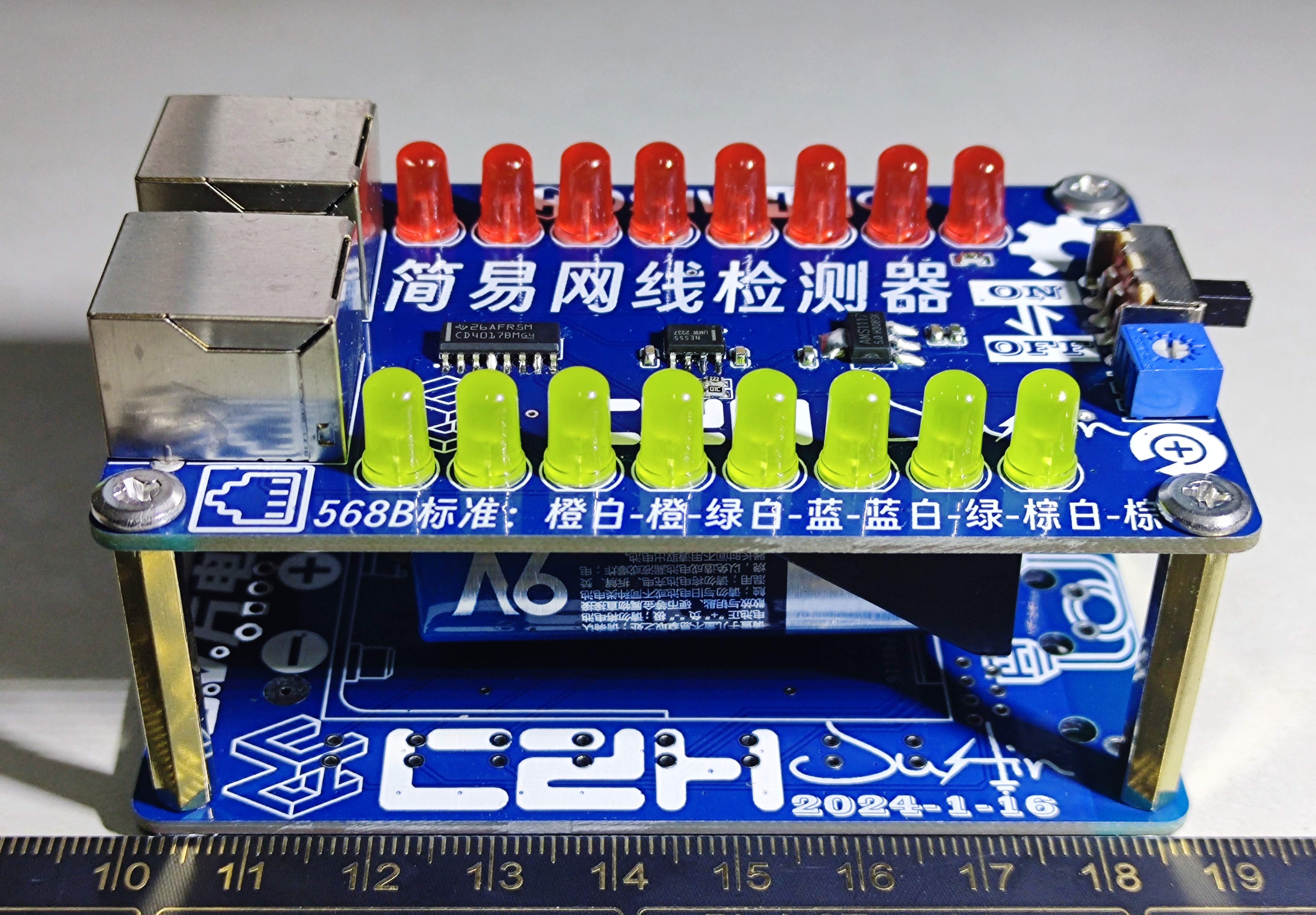
Sometimes I crimp network cables to make them. To facilitate testing the crimping contact, I replicated a simple network cable detector. For portability, I changed
the power supply from USB to battery. Power Supply Scheme 1: Boost – Two AA batteries 3V + Boost DC-DC = 5V Scheme 2: Buck – One 9V battery + LDO = 5V Because the NE555 requires Vmin = 4.5V, I didn't want to use three batteries, so I used a 9V battery and used an LDO to step down to 5V, minimizing external components. 9V batteries are also readily available. Due to low usage frequency and low power consumption, rechargeable lithium batteries were not used to save costs. A 0.1uF capacitor was added to the CONT of the NE555 for grounding, increasing anti-interference stability. Add a 51Ω LED current-limiting resistor. Note the forward voltage drop of the LED. The CD4017 outputs a high level of 4.95V. The two LEDs are connected in series via a network cable. Red and yellow LEDs (from stock) with a lower voltage drop of 2.2V are used here. Because a battery needs to be placed on the back, the IC resistors and capacitors are changed to surface-mount packages. --------------------------------------------------------------------------------- After the first version is tested, an additional power indicator light is added . Although the battery clip has a foolproof design, attempting to install the battery will briefly result in reverse connection, so reverse connection protection for the battery is added. --------------------------------------------------------------------------------- AMS1117 Note that TAB is also VOUT; do not ground it arbitrarily! Please refer to the LDO manual. The AMS1117 package was mistakenly purchased as SOT89; the correct package is SOT-223. (Actually, the larger package was initially mistakenly placed directly from the stock, but heat dissipation should be better.) --------------------------------------------------------------------------------- Low installation cost; no casing design is provided. The PCB and copper pillars are used for fixing. M3*28×4 copper pillars and M3 flathead screws×4 are used. The battery holder is directly fixed with hot melt glue, saving screws. --------------------------------------------------------------------------------- LED voltage drop and current parameters for different colors (ehaoan.com) : Through-hole super bright LEDs have three main colors with different voltage drops, as follows: Red LED voltage drop 2.0-2.2 V; Yellow LED voltage drop 1.8-2.0 V; Green LED voltage drop 3.0-3.2 V. The rated current during normal illumination is 20mA. --------------------------------------------------------------------------------- Surface mount LED voltage drop: Red 1.82-1.88V, current 5-8mA (generally calculated as 1.8V and 5mA, connected to 3.3V). Power supply current limiting resistors are typically connected to 470Ω (5V) or 680Ω. Green resistors are 1.75-1.82V, 3-5mA ; Orange resistors are 1.7-1.8V, 3-5mA; Blue resistors are 3.1-3.3V, 8-10mA; White resistors are 3-3.2V, 10-15mA. --------------------------------------------------------------------------------- (For simple path testing, the following design considerations can be ignored.) RJ45 Network PCB Layout Design Considerations: The RJ45 chassis ground and digital ground are isolated by a 1M ohm resistor and a 0.1uF decoupling capacitor. The spacing between the chassis ground and digital ground must be wider than 60mil. Author: Fanyi Education https://www.bilibili.com/read/cv6448110/ Source: bilibili --------------------------------------------------------------------------------- Key Points for LDO Power Supply PCB Design: 1. Analyze the power input and output. The layout should be either a straight line or an L-shape. The smaller the power loop, the better. 2. Input and output filter capacitors should be placed in order of size, from largest to smallest. 3. The number of power channels and vias must meet current carrying requirements. 4. Power input vias should be placed before the first filter capacitor, and power output vias should be placed after the last filter capacitor. 5. The GND current carrying path should be sufficiently wide, and vias should be uniformly placed close to the chip's GND pin. 6. Input ground and output ground should be connected together to ensure good return current. https://zhuanlan.zhihu.com/p/665866367


 京公网安备 11010802033920号

 177-710-5-31CS8J7-24MAN


