The
oscilloscope implementation requirements are:
±10V dual-channel 2M sampling rate or higher, 20k bandwidth
sine wave peak-to-peak measurement error no greater than 5%,
range switching function (switching control method is not limited)
, stable triggering, no obvious slippage
frequency measurement error no greater than 5%
, ±4V 20k output, square wave, triangle wave
, sine wave, and sine wave peak-to-peak error no greater than 15%.
This
project is based on the STM32H750 core board from Hardwood Classroom. For secondary development and design, attention should be paid to the I/O port allocation.
The schematic diagram design should explain
the specific allocation of the microcontroller's I/O ports and peripherals.

The following two figures show the power supply design. This design uses a 6-pin Type-C interface for power supply.
Note: When soldering the power supply section, pay attention to the pin network allocation, especially the selection of the three LDO models, otherwise there is a risk of smoke. Also, the power supply section is isolated from other parts. When soldering the power supply section, be careful not to have cold solder joints; check it first, and continue only after confirming there are no errors.


The following is the detailed design of the two input channels of this oscilloscope. For a better understanding of the principles, please refer to the open-source project on Hardwood Classroom. Here, I'll share some issues you might encounter:
1. During the project, most people choose to directly copy the schematic from Hardwood Classroom. This results in numerous op-amps appearing when updating the PCB (a chip only uses one of the four channels). I suggest deleting the original op-amp and placing it separately.
2. I also encountered some issues with the relay section in this project. Early on, I didn't fully understand the functions of each part of the schematic, leading to incorrect pin placement for the NO and NC networks of the three relays. This resulted in the finished product failing to input and output signals correctly (the problem was finally solved by using jumper wires).
3. The finished product may have a VPP value greater than the input voltage by 10V. You can try removing all the NC capacitors from the two oscilloscope channels.
4. Be restrained in using flux during soldering. Use it only when necessary; don't blindly apply a lot of flux to the pads, as this can cause short circuits. After using flux, clean it with a brush, or use board cleaner to clean the board. This makes it cleaner and easier to observe other components.
5. This project has verified that if problems occur, soldering issues account for 90%. Then check your schematic for errors
! I suggest drawing your own schematics, not acting as a CV engineer. Try to understand the principles of each part during the drawing process; this will greatly improve the efficiency of debugging and troubleshooting later.


shi-bo-qi Code.zip
Oscilloscope.mp4
Oscilloscope2.mp4
PDF_Simple Digital Oscilloscope Based on STM32H750.zip
Altium_Simple Digital Oscilloscope Based on STM32H750.zip
PADS_Simple Digital Oscilloscope Based on STM32H750.zip
BOM_Simple Digital Oscilloscope Based on STM32H750.xlsx
97158
Digital oscilloscope
Using the STM32H750 as the main control chip, this system implements the functions of a dual-channel oscilloscope and a single-channel signal generator.

Top view ,

bottom view,

square wave,

sine wave

, triangle wave

PDF_DigitalOscilloscope.zip
Altium Digital Oscilloscope.zip
PADS_DigitalOscilloscope.zip
BOM_DigitalOscilloscope.xlsx
97159
DSO and DDS based on STM32H750
The MCU is integrated with the oscilloscope, DDS analog front-end, power supply, etc., and features such as TF card, WIFI, and Bluetooth are added.
Preface to a Simple Oscilloscope and Signal Generator Based on STM32H750
I've always wanted to build a simple oscilloscope to fully learn the hardware and software development process. Last month, I was fortunate enough to see this training camp held by LCSC and excitedly participated.
Although I was too busy with work to rewrite the software design from scratch, I gained a lot in hardware design. I'm setting a goal here to definitely complete the software design of an oscilloscope myself.
Hardware Circuit
Because this is a simple oscilloscope, all the examples in this training camp are only small-scale signal input detection. The hardware circuit has been greatly simplified. However, I believe that a deeper understanding of this hardware circuit, and the ability to apply the knowledge to other situations, will definitely enrich our circuit knowledge. The


positive and negative power supplies for the op-amp section are provided by this part.
We are all familiar with the MT3608 BOOST circuit, but adding two diodes and two capacitors to generate a negative voltage is quite advanced. Currently, it's too messy, so the circuit has been simplified. The circuit shown in the


left box is a simplified BOOST section, which will not be analyzed here. Let's look at the circuit in the right box. Because the high-speed switching of the switch on the left side turns the power supply on the left side of C92 into a pulse signal. When the signal goes from low to high, the capacitor C92 charges (left +, right -). When the signal goes from high to low, the left side of C92 becomes 0 volts, but the voltage difference across the capacitor cannot change abruptly, causing the voltage on its right side to become -V. This allows the current to flow through GND->C91->D6->C92->GND. The final result is that the voltage at the positive terminal of D6 is a negative voltage slightly higher than -V.
Later, when I searched for relevant information online, I found that the structure of the block diagram on the right is a typical charge pump circuit, where energy transfer relies on the voltage difference of the capacitors. Because the current that can be provided is generally relatively small, around tens of milliamps, it is usually used as a power supply for simple op-amps.


This is the 3.3V power supply of my system, which includes both the switching power supply and the LDO. In actual soldering, I only soldered the switching power supply.


In my initial version, I only made a jumper to 3.3V for the signal relay power supply, but the signal relay I bought was a 5V power supply specification, which was a careless oversight. Therefore, two power supply options were added here.


The official documentation for the oscilloscope's analog front-end clearly explains attenuation, gain, DC bias, and comparator triggering.
Currently, the STM32H750VBT6 chip costs only around 20, so I chose to integrate the chip directly without borrowing a development board. Also, considering that the DSO, DDS, LCD, buttons, and relays don't use many pins, it would be a waste to leave the remaining pins unused. To increase its versatility,


I added some peripherals to the board, such as a TF card for expanding waveform capture functionality; QSPI for external FLASH; and KT6368A Bluetooth and ESP8266WIFI for remote control and display. For the remaining pins, I chose the Raspberry Pi expansion interface, which has the most compatible modules, allowing for easy direct connection of various modules. To simplify layout and routing, I modified some interface pins
in the software ; the modified pins are shown below. For ordinary I/O, only the pins need to be modified. It's important to note that when modifying SPI, the priority of the SPI transmission interrupt and DMA transmission interrupt should not be too high, otherwise, a freeze may occur. Regarding saving waveforms on the SD card, I initially planned to save the waveforms as BMP images, as shown in the screenshot taken at the beginning. However, when I tried to take screenshots during runtime, it froze. I currently suspect this is due to the blocking mode used for writing and reading from the TF card, which is frequently interrupted by the ADC interrupt. I will try switching to DMA mode later. This function is not yet complete. The flying wire in the lower right corner is related to the relay power supply issue mentioned earlier (already modified in the PCB). The flying wire in the upper left corner is because the 3225 package crystal oscillator I purchased cannot power the Bluetooth chip, so I used the included 2-pin crystal oscillator for testing. Later, there is a video showing the ADC DMA buffer data being uploaded to the VOFA+ display via the Bluetooth transparent serial port. The ESP8266 is not yet soldered because I am still learning about network-related operations and knowledge. Once I learn, I will complete this part and create some fun functions. That's about it for now, a summary of my progress in participating in this training camp in my spare time. The code is on GitHub; feel free to follow it if you're interested. I will update it if new features are developed (if I have time). https://github.com/starry-m/H750_ADCDAC.git Future Plans and Ideas Functionality Completion Status Screenshots (To be completed ) Host Computer Display and Control (Bluetooth) (To be completed ) USB Simulated USB Flash Drive Firmware Upgrade (To be completed) WIFI Control (To be completed ) Although I'm still far from my goal of building a complete oscilloscope, this training camp experience allowed me to go through the design and drawing of hardware circuits, which is not bad. Problem Log The downloader can run after downloading, but the screen does not display after resetting and powering on . Solution: It should be due to unstable power supply during startup; a 1-second delay before startup resolves the issue and allows for normal display.


DAC.bin
DAC.hex
source code.zip
Demo.mp4
PDF_DSO and DDS based on STM32H750.zip
Altium-based DSO and DDS using STM32H750.zip
PADS_DSO and DDS based on STM32H750.zip
BOM_DSO and DDS based on STM32H750.xlsx
97160
Issue 13, 2023 - Portable USB Power Meter Based on CW32
I have a lot of gadgets around me, like USB lights, USB fans, and USB humidifiers, so I wanted to make a simple power meter. It doesn't need to be extremely precise, but at least I need to know roughly how many volts and milliamps it is. Isn't that easy? If you feel the same way, then go ahead and make a copy!
Preface:
Before starting, I was full of confidence, thinking this little gadget would be a piece of cake!
But after starting, I was completely outmaneuvered. It really proved Li Gong's words true: this thing isn't difficult in theory, but doing it well is not easy at all.
To make it truly precise is indeed very difficult, especially current measurement, which I'll discuss later.
In short, the simpler something looks, the more difficult it is to do.
Finally, thank you to all the experts, and thank you to LCSC for giving me this opportunity. This was the most memorable project for me; there were so many pitfalls.
Principle Introduction
: A power meter calculates the power consumption of electronic products. It's usually measured in watts or milliwatts.
Two data points need to be measured: first, voltage u, which is the voltage drop;
second, current i.
Therefore, power P = u * i. The principle is that simple.
It looks simple, but doing it is not.
Hardware Design:
The following will introduce the entire circuit in sections.
The main control chip
chosen this time is the CW32F030C8T6. This ARM M0 core chip features the following characteristics:
• Core: ARM® Cortex®-M0+
with a maximum clock speed of 64MHz
• Operating temperature: -40℃ to 105℃; Operating voltage: 1.65V to 5.5V
• Storage capacity
: Maximum 64KB FLASH, data retention for 25 years @ 85℃;
Maximum 8KB RAM with parity support;
128KB OTP memory •
CRC hardware calculation unit;
Reset and power management:
Low-power modes (Sleep, DeepSleep)
; Power-on and power-down reset (POR/BOR);
Programmable low-voltage detector (LVD)
• Clock management:
4 ~ 32MHz crystal oscillator;
32kHz low-speed crystal oscillator;
Built-in 48MHz RC oscillator;
Built-in 32kHz RC oscillator
; Built-in 10kHz RC oscillator; Built
-in 150kHz RC oscillator;
Built-in PLL phase-locked
loop clock monitoring system
allows independent shutdown of peripheral clocks
• Supports up to 39 I/O interfaces;
All I/O... This chip features interrupt support
for all I/O ports, interrupt input filtering,
a five-channel DMA controller , a 12-bit analog-to-digital
converter with ±1 LSB and a maximum 1M SPS conversion speed, a built-in voltage reference, an analog watchdog function , a built-in temperature sensor , dual voltage comparators , a real-time clock and calendar with sleep/deep-sleep wake-up mode , a 16-bit advanced control timer supporting 6 capture/compare channels and 3 pairs of complementary PWM outputs, dead time, and flexible synchronization, four 16-bit general-purpose timers, three 16-bit basic timers, a window watchdog timer , and an independent watchdog timer . Communication interfaces include three low-power UARTs supporting fractional baud rates, two SPI interfaces (12 Mbit/s), two I2C interfaces (1 Mbit/s) , an IR modulator, and a serial debug interface (SWD). This chip boasts low power consumption, various packages, is domestically produced, and is offered at a competitive price; it's a highly recommended choice. This project uses few pins, mainly controlling the following interfaces : ADC: power and current serial port; debugging and printing; IIC: control of the display screen schematic is as follows: Although the power supply section uses a USB power meter, considering the possibility of measuring larger voltages, an LDO was chosen, supporting a maximum input of 12V. This is generally sufficient. Output is 3.3V, maximum 800mA. This is also for future use with multiple fixed 3.3V output voltage modules. Therefore, the overall measured voltage should not exceed 12V. The specific implementation schematic is as follows: The display screen uses a 0.91-inch white text screen. 128x32, it can display four lines. The interface and dimensions are as follows: This is modular, the internal circuit is as follows, the IIC does not require pull-up resistors, the module has them built-in. It works very well. Therefore, the schematic design of this project only needs to reserve interfaces, as shown below: For cost savings, a voltage divider circuit is directly used in the voltage acquisition circuit, as shown in the diagram below . Note: The CW32 community suggests adding a resistor to the VADC. Personally, I think if you have the budget, you can use an operational amplifier circuit or a voltage follower circuit to improve driving capability and reduce impedance. This is just my personal suggestion. The VADC uses PA1 for sampling. The current acquisition circuit generates a voltage drop by connecting a small resistor in series. Then, the TI chip INA199A3DCKR is used as a dedicated current sensing amplifier. There are three options; I chose the 200x one. If you are measuring small currents, choose the 50x or 100x one. The corresponding models are as follows: I chose the 200x A3, which uses a reference voltage of 2.5V with the CW32 ADC. This is the internal configuration of the CWF030; there are also 3.3V and 1.5V options available, but I chose 2.5V. Therefore, the maximum current Imax = 2.5/200/0.01 = 1.25A. For commonly used computer USB ports, this value is sufficient. If you find it too high or too low, you can choose different amplifiers with different voltage references. For example, if I choose 3.3V, then Imax = 1.65A, which will not be accurate for testing small currents. The smaller the range, the more accurate the measurement; please refer to this rule. *Based on the previous maximum voltage of 12V, the load power Pmax = 121.25 = 15W. It absolutely cannot be higher. Higher values may cause smoke. ** The principle design is as follows: **


The indicator lights
here use colored LEDs, specifically the WS2812, which is quite popular and cool recently.
The circuit is very simple, as shown below. The driver hasn't been written yet; I'll update the software in the second version.

Regarding the other download, reset, and mode circuits , I'll only discuss the reset circuit here. Due to DAP debugging, a soft reset
isn't possible, so it's best to leave a hardware reset interface or connect it directly to the downloader's RST; otherwise, it's quite troublesome.
The specific schematic is as follows:

The software implementation
will also be explained in several parts. The display part mainly involves the IIC driver; for SSD106, simply refer to the official initialization function. The flowchart is as follows . The OLED initialization function is as follows: As for using text or images, we can use image extraction software. The detailed code is too long to paste here. You can refer to the relevant functions. The ADC acquisition part uses pins PA1 and PA2 to acquire voltage and current respectively. If related files need modification, it's best to refer to the manual and write your own; this is suitable for direct replication. I spent too much time on this part, encountering various errors and pitfalls. In short, please take it seriously. The relevant configuration functions are as follows: ifndef __ADC_H define __ADC_H ifdef __cplusplus extern "C" { endif / Includes ------------------------------------------------------------------/ include "base_types.h" include "cw32f030.h" include "system_cw32f030.h" include "interrupts_cw32f030.h" include "cw32f030_systick.h" include "cw32f030_rcc.h" include "cw32f030_gpio.h" include "cw32f030_adc.h" extern uint16_t gAdcResult[4]; void ADC_Config(void); uint8_t Gain_Value(void); ifdef __cplusplus } endif endif / __ADC_H / The implementation file of adc.c is as follows: /** Include files **/include "adc.h" /** Local pre-processor symbols/macros ('#define') **/ / USER CODE BEGIN EM / / Sequence channel continuous sampling mode/ //#define SQR_CONTINUOUS_MODE_EN / Sequence channel scan sampling mode/ define SQR_SCAN_MODE_EN / Sequence channel multiple sampling mode/ //#define SQR_MORE_MODE_EN / Sequence channel discontinuous sampling mode/ //#define SQR_BREAK_MODE_EN / USER CODE END EM / /** Global variable definitions (declared in header file with 'extern') **/ /** Local type definitions ('typedef') **/ /** Local function prototypes ('static') **/ /** Local variable definitions ('static') * **/ uint16_t valueAdc; uint16_t gAdcResult[4]; uint32_t valueAdcAcc; volatile uint8_t gFlagIrq; uint16_t gCntEoc = 0; uint8_t cntSample; /** Local pre-processor symbols/macros ('#define') **/ /***** Function implementation - global ('extern') and local ('static') **/ /** @brief ADC I/O initialization */ void ADC_PortInit(void) { // Enable GPIO clock REGBITS_SET(CW_SYSCTRL->AHBEN, SYSCTRL_AHBEN_GPIOA_Msk); // Enable ADC clock REGBITS_SET(CW_SYSCTRL->APBEN2,SYSCTRL_APBEN2_ADC_Msk); //set PA01 as AIN1 INPUT PA01_ANALOG_ENABLE();


//set PA02 as AIN2 INPUT
PA02_ANALOG_ENABLE();
// //set PA05 as AIN5 INPUT
// PA06_ANALOG_ENABLE();
// //set PA07 as AIN7 INPUT
// PA07_ANALOG_ENABLE();
}
void ADC2_Config(void)
{
ADC_InitTypeDef ADC_InitStructure;
ADC_SerialChTypeDef ADC_SerialChStructure;
//Configure ADC test I/O port
ADC_PortInit();
//ADC initialization
// ADC_InitStructure.ADC_SampleTime=ADC_SampTime10Clk;
// ADC_InitStructure.ADC_VrefSel=ADC_Vref_BGR1p5;
ADC_StructInit(&ADC_InitStructure);
//ADC working clock configuration
ifdef SQR_BREAK_MODE_EN
ADC_InitStructure.ADC_ClkDiv = ADC_Clk_Div1;
else
ADC_InitStructure.ADC_ClkDiv = ADC_Clk_Div16;
endif
// ADC sequence scan conversion mode configuration
ADC_SerialChStructure.ADC_Sqr0Chmux = ADC_SqrCh1;//ADC_SqrVddaDiV3; //ADC_SqrCh1;
ADC_SerialChStructure.ADC_Sqr1Chmux = ADC_SqrCh2; //ADC_SqrCh2; //
// ADC_SerialChStructure.ADC_Sqr2Chmux = ADC_SqrCh6; //ADC_SqrCh5;
// ADC_SerialChStructure.ADC_Sqr3Chmux = ADC_SqrCh7;
ADC_SerialChStructure.ADC_SqrEns = ADC_SqrEns01;
ADC_SerialChStructure.ADC_InitStructure = ADC_InitStructure;
ifdef SQR_CONTINUOUS_MODE_EN
/ Serial channel continuous sampling mode /
ADC_SerialChContinuousModeCfg(&ADC_SerialChStructure);
ADC_ITConfig(ADC_IT_EOS, ENABLE);
elif defined (SQR_SCAN_MODE_EN)
/ Serial channel scan sampling mode /
ADC_SerialChScanModeCfg(&ADC_SerialChStructure);
ADC_ITConfig(ADC_IT_EOS, ENABLE);
elif defined (SQR_MORE_MODE_EN)
/ Serial channel multiple sampling mode /
cntSample = 0xFF; // Conversion count is 0xFF + 1.
ADC_SerialChMoreModeCfg(&ADC_SerialChStructure, cntSample);
ADC_ITConfig(ADC_IT_EOC | ADC_IT_EOA, ENABLE);
elif defined (SQR_BREAK_MODE_EN)
/ Serial channel intermittent sampling mode /
ADC_SerialChBreakModeCfg(&ADC_SerialChStructure);
ADC_ITConfig(ADC_IT_EOC | ADC_IT_EOS, ENABLE);
else
error "Please select ADC's running mode first in main.h!"
endif
//ADC_ITConfig(ADC_IT_EOC | ADC_IT_EOS | ADC_IT_EOA, ENABLE);
ADC_EnableIrq(ADC_INT_PRIORITY);
ADC_ClearITPendingAll();
//ADC enable
ADC_Enable();
ADC_SoftwareStartConvCmd(ENABLE);
}
uint8_t Gain2_Value(void)
{
uint8_t temp=0;
ifdef SQR_CONTINUOUS_MODE_EN
/ Serial channel continuous sampling mode /
while (!(gFlagIrq & ADC_ISR_EOS_Msk));
gFlagIrq = 0u;
//while(!(gFlagIrq & ADC_ISR_EOS_Msk));
ADC_GetSqr0Result(gAdcResult);
ADC_GetSqr1Result(&gAdcResult[1]);
// ADC_GetSqr2Result(&gAdcResult[2]);
// ADC_GetSqr3Result(&gAdcResult[3]);
//printf("ch1:%5d-ch2:%5d-ch6:%5d-ch7:%5d
",gAdcResult[0],gAdcResult[1],gAdcResult[2],gAdcResult[3]);
elif defined (SQR_SCAN_MODE_EN)
/ Sequence channel scan sampling mode /
while (!(gFlagIrq & ADC_ISR_EOS_Msk));
gFlagIrq = 0u; ADC_GetSqr0Result (gAdcResult); ADC_GetSqr1Result(&gAdcResult[1]); //
ADC_GetSqr2Result (&gAdcResult[2]); //
ADC_GetSqr3Result(&gAdcResult[3]); //printf("ch1:%5d-ch2:%5d-ch6:%5d-ch7:%5d ",gAdcResult[0], gAdcResult[1],gAdcResult[2], ...3]); //printf("ch1:%5d-ch2:%5d-ch6:%5d-ch7:%5d " ,gAdcResult[3]); //printf("ch1:%5d-ch2:%5d-ch6:%5d-ch7:% ",gAdcResult[0],gAdcResult[1],gAdcResult[2],gAdcResult[3]); elif defined (SQR_MORE_MODE_EN) / Sequence channel multiple sampling mode/ while (!(gFlagIrq & ADC_ISR_EOA_Msk)); gFlagIrq = 0u; ADC_GetSqr0Result(gAdcResult); //Get data. ADC_GetSqr1Result(&gAdcResult[1]); // ADC_GetSqr2Result(&gAdcResult[2]); // ADC_GetSqr3Result(&gAdcResult[3]); ADC_GetAccResult(&valueAdcAcc); if (gCntEoc != (cntSample + 1)) { temp=1; } //printf("ch1:%5d-ch2:%5d-ch6:%5d-ch7:%5d ",gAdcResult[0],gAdcResult[1],gAdcResult[2],gAdcResult[3]); gCntEoc = 0u; elif defined (SQR_BREAK_MODE_EN) / Sequence channel intermittent sampling mode/ while (!(gFlagIrq & ADC_ISR_EOC_Msk)); gFlagIrq &= (~ADC_ISR_EOC_Msk); if (gFlagIrq & ADC_ISR_EOS_Msk) { gFlagIrq = 0u; ADC_GetSqr0Result(gAdcResult); ADC_GetSqr1Result(&gAdcResult[1]); // ADC_GetSqr2Result(&gAdcResult[2]); // ADC_GetSqr3Result(&gAdcResult[3]); //printf("ch1:%5d-ch2:%5d-ch6:%5d-ch7:%5d ",gAdcResult[0],gAdcResult[1],gAdcResult[2],gAdcResult[3]); } endif ifndef SQR_CONTINUOUS_MODE_EN ADC_SoftwareStartConvCmd(ENABLE); //Start the next ADC conversion endif return temp; } Serial port output implementation To facilitate debugging, serial port 1, print output, etc. are implemented. The implementation function is as follows: /** Include files **/include "uart1.h" /** Local pre-processor symbols/macros ('#define') **/ //UARTxdefine DEBUG_USARTx CW_UART1 define DEBUG_USART_CLK RCC_APB2_PERIPH_UART1 define DEBUG_USART_APBClkENx RCC_APBPeriphClk_Enable2 define DEBUG_USART_UclkFreq 8000000 //UARTx GPIO define DEBUG_USART_GPIO_CLK RCC_AHB_PERIPH_GPIOA define DEBUG_USART_TX_GPIO_PORT CW_GPIOA define DEBUG_USART_TX_GPIO_PIN GPIO_PIN_8 define DEBUG_USART_RX_GPIO_PORT CW_GPIOA define DEBUG_USART_RX_GPIO_PIN GPIO_PIN_9 //GPIO AF define DEBUG_USART_AFTX PA08_AFx_UART1TXD() define DEBUG_USART_AFRX PA09_AFx_UART1RXD() /** Local variable definitions ('static') * **/ifdef __GNUC__
/ With GCC/RAISONANCE, small printf (option LD Linker->Libraries->Small printf
set to 'Yes') calls __io_putchar() /
define PUTCHAR_PROTOTYPE int __io_putchar(int ch)
else
define PUTCHAR_PROTOTYPE int fputc(int ch, FILE *f)
endif / __GNUC__ /
/**
Local pre-processor symbols/macros ('#define')
**/
/**
@brief Retargets the C library printf function to the USART.
*/
PUTCHAR_PROTOTYPE
{
USART_SendData_8bit(DEBUG_USARTx, (uint8_t)ch);
while (USART_GetFlagStatus(DEBUG_USARTx, USART_FLAG_TXE) == RESET);
return ch;
}
/**
@brief Configure GPIO
*/
void UART1_GPIO_Configuration(void)
{
GPIO_InitTypeDef GPIO_InitStructure;
RCC_AHBPeriphClk_Enable(DEBUG_USART_GPIO_CLK, ENABLE);
DEBUG_USART_APBClkENx(DEBUG_USART_CLK, ENABLE);
//UART TX RX multiplexing
DEBUG_USART_AFTX;
DEBUG_USART_AFRX;
GPIO_InitStructure.Pins = DEBUG_USART_TX_GPIO_PIN;
GPIO_InitStructure.Mode = GPIO_MODE_OUTPUT_PP;
GPIO_InitStructure.Speed = GPIO_SPEED_HIGH;
GPIO_Init(DEBUG_USART_TX_GPIO_PORT,&GPIO_InitStructure)
;
GPIO_InitStructure.Mode = GPIO_MODE_INPUT_PULLUP;
GPIO_Init(DEBUG_USART_RX_GPIO_PORT, &GPIO_InitStructure);
}
/**
@brief Configure UART
*/
void UART1_Configuration(uint32_t BaudRate)
{
USART_InitTypeDef USART_InitStructure;
USART_InitStructure.USART_BaudRate = BaudRate;
USART_InitStructure.USART_Over = USART_Over_16;
USART_InitStructure.USART_Source = USART_Source_PCLK;
USART_InitStructure.USART_UclkFreq = DEBUG_USART_UclkFreq;
USART_InitStructure.USART_StartBit = USART_StartBit_FE;
USART_InitStructure.USART_StopBits = USART_StopBits_1;
USART_InitStructure.USART_Parity = USART_Parity_No ;
USART_InitStructure.USART_HardwareFlowControl = USART_HardwareFlowControl_None;
USART_InitStructure.USART_Mode = USART_Mode_Rx | USART_Mode_Tx;
USART_Init(DEBUG_USARTx, &USART_InitStructure);
}
/**
@brief Send an 8-bit array
@param USARTx : USARTx peripheral
parameters can be:
CW_UART1, CW_UART2, CW_UART3
@param TxBuf : The array to be sent
@param TxCnt : The number of array elements to be sent
/
void UART1_SendBuf_Polling(uint8_t TxBuf, uint8_t TxCnt)
{
while (TxCnt)
{
USART_SendData_8bit(CW_UART1, *TxBuf);
while (USART_GetFlagStatus(CW_UART1, USART_FLAG_TXE) == RESET);
TxBuf++;
TxCnt--;
}
while (USART_GetFlagStatus(CW_UART1, USART_FLAG_TXBUSY) == SET);
}
/**
@brief Receive 8-bit array
@param USARTx : USARTx peripheral
parameters can be:
CW_UART1, CW_UART2, CW_UART3
@param RxBuf : Receive Buf
@return uint8_t : Number of characters received
/
uint8_t UART1_RecvBuf_Polling(uint8_t RxBuf)
{
uint8_t RxCnt = 0;
do
{
//Wait for RC
while (USART_GetFlagStatus(CW_UART1, USART_FLAG_RC) == RESET);
//Clear RC
USART_ClearFlag(CW_UART1, USART_FLAG_RC);
//ERROR: PE or FE
if (USART_GetFlagStatus(CW_UART1, USART_FLAG_PE | USART_FLAG_FE))
{
USART_ClearFlag(CW_UART1, USART_FLAG_PE | USART_FLAG_FE);
RxCnt = 0x00;
}
else
{
RxBuf[RxCnt] = USART_ReceiveData_8bit(CW_UART1);
RxCnt++;
}
}
while (RxBuf[RxCnt - 1] != '
');
return RxCnt;
}
The effect is as follows:

The main control function
executes in the following order:
First, it initializes various configurations, such as clock, GPIO, serial port, and screen configuration.
Then, it performs data acquisition and screen refresh in a loop, with a 500ms delay function added in between.
The specific code is as follows:
/**/
/ file main.c
A detailed description is available at
@link Sample Group Some description @endlink
- 2021-03-12 1.0 xiebin First version for Device Driver Library of Module.
****/
/***
Code License and Disclaimer Information
Wuhan Xinyuan Semiconductor Co., Ltd. grants you a non-exclusive copyright license to use all programming code examples, from which you can
generate similar functions customized to your specific needs. Subject to any statutory warranties that cannot be excluded, Wuhan Xinyuan
Semiconductor Co. Ltd., its program developers, and suppliers make no express or
implied warranties or conditions regarding the program or technical support (if any), including but not limited to implied warranties
or conditions of merchantability, fitness for a particular purpose, and non-infringement.
In no event shall Wuhan Xinyuan Semiconductor Co., Ltd., its program developers, or suppliers be liable for any of the following,
even if advised of the possibility of their occurrence: loss or damage to data; direct, special, incidental
, or indirect damages, or any consequential economic damages; or loss of profits, business, revenue, goodwill, or anticipated savings
.
Some jurisdictions do not allow any exclusions or limitations on direct, incidental, or consequential damages, so some or
all of the above exclusions or limitations may not apply to you.
***/
/**
Include files
**/include "main.h"
/**
Local pre-processor symbols/macros ('#define')
**/
/**
Global variable definitions (declared in header file with 'extern')
**/
extern uint16_t gAdcResult[4];
/**
Local type definitions ('typedef')
**/
/**
Local function prototypes ('static')
**/
/**
Local variable definitions ('static') *
**/
uint8_t TxRxBufferSize;
uint8_t TxRxBuffer[] = "
CW32F030 UART Polling
";
/**
Local pre-processor symbols/macros ('#define')
**/
/*****
Function implementation - global ('extern') and local ('static')
**/
/**
rief Main function of project
eturn uint32_t return value, if needed
**/
int32_t main(void)
{
uint8_t flag=0;
float x,y,z;
//char s[20];
//SYSCLK = HSI = 8MHz = HCLK = PCLK
RCC_HSI_Enable(RCC_HSIOSC_DIV6);
//Configure GPIO
UART1_GPIO_Configuration();
//Configure UART
UART1_Configuration(9600);
OLED_Init(); //Initialize OLED
OLED_Clear();
OLED\_ShowString(20,1,"My Power Calc",8,1);//6*8
UART1_SendBuf_Polling(TxRxBuffer, ARRAY_SZ(TxRxBuffer) - 1);
for(uint8_t i=0;i<3;i++)
{
delay1ms(500);
printf("hello kwin
");
}
ADC2_Config();
while (1)
{
char s[20];
flag=Gain2_Value();
if(!flag)
{
printf("
ch1:%5d-ch2:%5d-ch6:%5d-ch7:%5d
",gAdcResult[0],gAdcResult[1],gAdcResult[2],gAdcResult[3]);
//printf("ch1:%5d
",gAdcResult[0]);
x=gAdcResult[0]/4095.025;
sprintf(s,"U=%6.3fV",x);
printf("
U=%6.3fV
",x);
OLED_ShowString(40,9,s,8,1);//68
//printf("ch2=%5d
",gAdcResult[1]);
y=gAdcResult[1]/4095.01.25;
sprintf(s,"I=%6.3fA",y);
printf("I=%6.3fA
",y);
OLED_ShowString(40,17,s,8,1);//68
z=xy;
sprintf(s,"P=%6.3fW",z);
OLED_ShowString(40,25,s,8,1);//68
}else{printf("Get Value failed
");}
OLED\_DrawLine(0,0,127,0,1);
OLED\_DrawLine(127,0,127,31,1);
OLED\_DrawLine(0,0,0,31,1);
OLED\_DrawLine(0,31,127,31,1);
OLED\_DrawLine(0,31,127,31,1);
//OLED\_DrawCircle(63,31,16);
OLED_Refresh();
delay1ms(500);
}
}
/**
@brief Configure RCC
*/
/**
EOF (not truncated)
**/ifdef USE_FULL_ASSERT
/**
@brief Reports the name of the source file and the source line number
where the assert_param error has occurred.
@param file: pointer to the source file name
@param line: assert_param error line source number
@retval None
/
void assert_failed(uint8_t file, uint32_t line)
{
/ USER CODE BEGIN 6 /
/ User can add his own implementation to report the file name and line number,
tex: printf("Wrong parameters value: file %s on line %d
", file,line) /
/ USER CODE END 6 /
}endif / USE_FULL_ASSERT /
Test Results:
First, the voltage measurement: is quite accurate. I used a single measurement; averaging multiple measurements would yield better results, stabilizing at the mV level. Don't ask me how I know this; besides the code shown above, I have various incomplete versions, and I've conducted in-depth comparisons of accuracy.
Second, the current measurement: is not very accurate at 10 mA. Above 100 mA, the error is within 1%, and below 100 mA, it might be above 5%, varying considerably. Everyone is welcome to replicate this and conduct comparative experiments with electronic loads.
The overall power measurement is quite accurate, making it convenient for rough quantitative analysis.
Actual results are as follows:

Due to article length limitations, only the core code can be posted. However, the second version should be released soon.
Those in a hurry to replicate can use the attached .hex file. Contact me if you urgently need the source code; otherwise, please wait patiently for the second version update.
In summary,
this is my first encounter with the CW32 chip, and I have gained a preliminary understanding of it. In future work and studies, I will further learn about and apply domestically produced chips. Thanks to this platform and CW32. I hope domestically produced chips will continue to improve.
I'm going on a business trip tomorrow, so I finished this today (November 18, 2023, 19:18:00).
The hardware for the second board has arrived, but I won't have time to finish it before the deadline. There's still room for improvement in both software and hardware. Anyone interested can join me in DIY.
Making a PCB cover directly for the second version should yield better results. Why not print a shell? That's obvious, we're just too poor!

The PCB cover hasn't arrived yet, but here are some preview images on Bilibili: [


Links to Bilibili videos] (https://www.bilibili.com/video/BV1T94y1H7KJ/?pop_share=1&vd_source=e36622a05269c0356d6cd566056a2488 ) [Links to Bilibili videos]( https://www.bilibili.com/video/BV1MH4y1q7Wp/?pop_share=1&vd_source=e36622a05269c0356d6cd566056a2488 ) [Links to Bilibili videos] (https://www.bilibili.com/video/BV1MH4y1q7Wp/?pop_share=1&vd_source=e36622a05269c0356d6cd566056a2488 ) [Links to Bilibili videos] (https://www.bilibili.com/video/BV1La4y1U74q/?pop_share=1&vd_source=e36622a05269c0356d6cd566056a2488 )
No-load experiment.mp4
Loading Liangshan Sect.mp4
Desktop Humidifier Loading.mp4
Template.hex
PDF_Issue 13, 2023 - Portable USB Power Meter Based on CW32.zip
Altium_2023 Issue 13 - Portable USB Power Meter Based on CW32.zip
PADS_2023 Issue 13 - Portable USB Power Meter Based on CW32.zip
BOM_2023 Issue 13 - Portable USB Power Meter Based on CW32.xlsx
97161
51 microcontroller minimum system board and 51 programmer
Both the 51 microcontroller minimum system board and the 51 programmer can be programmed using DuPont wires and dual USB male connectors. Using USB for programming eliminates the need to connect the DuPont wires manually. We can directly plug the USB cable into the two female USB connectors on the minimum system board and the programmer for programming.
Introduction to the 51 Microcontroller Minimum System Board and 51 Programmer: I. 51 Microcontroller Minimum System Board: 1. It does not require an external power supply; 2. It can be used to program via DuPont wires or dual USB male connectors; II. 51 Programmer: 1. The programmer can be used to program via both DuPont wires and dual USB male connectors; 2. A self-locking switch needs to be pressed during programming (for a cold start). Feel free
to contact me if you need any!
DIY Ziyi Technology 51 Microcontroller Minimum System Board and 51 Downloader.mp4
PDF_51 Microcontroller Minimum System Board and 51 Downloader.zip
Altium_51 microcontroller minimum system board and 51 programmer.zip
PADS_51 Microcontroller Minimum System Board and 51 Downloader.zip
BOM_51 Microcontroller Minimum System Board and 51 Downloader.xlsx
97163
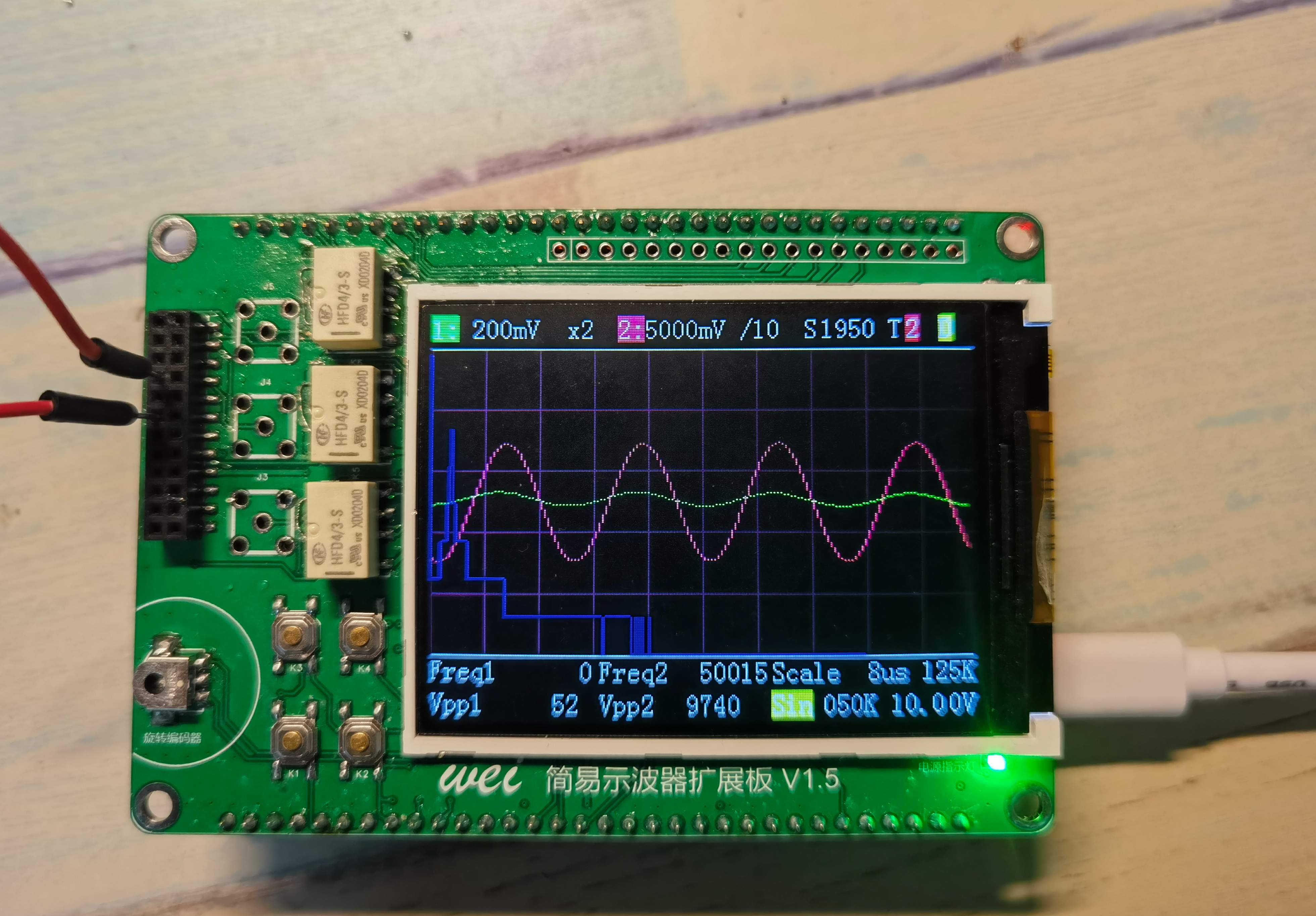
Instrument Training Camp: Portable Oscilloscope and H750 Core Board Replica
This is a replica of the portable oscilloscope from the LCSC + Hardwood Classroom Instrumentation Training Camp! It consists of two boards: an STM32H750 core development board and an oscilloscope expansion board. The core board can be used independently as a development board!
This is a replica of the portable oscilloscope from the LCSC + Hardwood Classroom Instrumentation Training Camp.
This project consists of two 4-layer boards:
1. H750 core board (copied from: https://oshwhub.com/micespring/stm32h750vb-CoreBoard_copy). Many unnecessary circuits have been removed, component packages have been changed to 0603 for easier soldering, and the pin headers have been redesigned to match the Hardwood Classroom H750 core board for easier connection to the oscilloscope motherboard. The core board can also be used as a standalone development board.
2. Oscilloscope expansion board: The schematic is copied from the course's example project, the screen interface has been moved to the core board, and the power interface has been changed to Type-C. This
is my first attempt at designing a 4-layer board, so there are bound to be many shortcomings!
The project still has some issues; I can't consistently measure the waveform of DAC_OUT using this oscilloscope. I don't know why.
I specifically built a PWM board for testing, and the input waveform can be measured.
Photos of JLCPCB 4-layer PCB:
H750 core board:


Oscilloscope expansion board:


3D Monkey 3D printed shell photos:


LCPCB online store panel printing photos:


The panel was exported from a PDF using an editor, converted to an image, and then imported into the panel editor. It was then drawn according to the positions of each component, but the result was too small, so it's just usable. There may have been errors during various conversions and imports; I must pay attention to checking the dimensions next time!
Photos of the soldered PCB:


The soldering order for the H750 core board was: first solder the Type-C interface and power supply; after testing the power supply and confirming it was working, then solder the STM32 main unit and peripheral circuits; after testing it again, write the main program; the third step was to solder the LED screen circuit, then test if the screen lit up; after it lit up, solder the other peripheral circuits and pin headers! The test passed completely!
The expansion board also started with soldering the power supply circuit; after testing and confirming it was working, soldered the other components!
Here's a pitfall to note regarding the expansion board's power supply section: the FB pin feedback circuit of the MT3608 must be correctly connected; otherwise, it will burn out the MT3608 chip upon power-on testing, causing a short circuit in the entire power supply circuit! I initially bought only one 3608 diode, then bought ten more. After using half of them and repeatedly disassembling and testing the peripheral components, I finally found the cause: I don't know if the D6 transient suppression diode from the original official project was faulty, or if the component I bought was faulty. This diode wasn't labeled with positive and negative terminals, and I might have connected it backwards, causing the feedback circuit to fail and burning out the chip!
Later, I tested D4 and D5, and the circuit using the same diode at -12V also didn't work properly. I replaced D4, D5, and D6 with SS34 diodes, and the circuit worked normally!
Regarding the core board, I initially didn't notice and bought a common cathode RGB LED from the 3528. After replacing it with a common anode LED, it lit up normally! Please be careful not to make the same mistake!
Assembly test photos:


Program writing:
There's not much to say about the program part. I used the original official program, installing KeilMDKARM5.35 and STM32H750 from the pack provided in the group file, version 2.7.0.
Because the official H750 pin header connectors PB8 and PB9 were incorrectly labeled, I didn't notice this when designing the core board, so these two pins were reversed. I modified the pin definitions during compilation, and it compiled successfully!
The modified relay.h file is shown in the image.

Since this H750 core board includes a USB interface, flashing the program was relatively simple. Open the STM32CubeProgrammer software, connect the core board to the computer using a Type-C data cable, press and hold the Boot button to power on the core board, adjust the USB connection in STM32CubeProgrammer, and then open the compiled DAC.hex file to download and flash the program.
DAC.hex
studio_video_1700182970550.mp4
VID_20231118_161821_0_COMPRESSED.mp4
PDF_Instrument Training Camp Portable Oscilloscope and H750 Core Board Replica.zip
Altium_Instrument Training Camp Portable Oscilloscope and H750 Core Board Replica.zip
PADS_Instrument Training Camp Portable Oscilloscope and H750 Core Board Replica.zip
BOM_Instrument Training Camp Portable Oscilloscope and H750 Core Board Replica.xlsx
97164
Heart-shaped flowing water lamp
This kit contains 18 red LEDs arranged in three groups to form a heart shape. Driven by a transistor oscillator circuit, the red heart shape rotates and flashes continuously in a clockwise direction, creating a dynamic effect, especially when used at night.
As shown in the schematic, the 18 LEDs are divided into 3 groups. When the power is turned on, the 3 transistors will compete to turn on, but due to differences in components, only one transistor will turn on first. Let's assume Q1 turns on first, then the group of LEDs 1 will light up. Because Q1 is on, its collector voltage drops, causing the voltage across capacitor C2 to drop to close to 0V. Since the voltage across a capacitor cannot change abruptly, the base of Q2 is also pulled to approximately 0V, and Q2 is cut off. Therefore, the group of LEDs connected to its collector is off. At this time, the high voltage of Q2 increases the collector voltage of Q3 through capacitor C3, and Q3 will also quickly turn on, lighting up the group of LEDs 3. Therefore, during this period, the collectors of Q1 and Q3 are both at a low level, and groups of LEDs 1 and 3 are lit, while group 2 is off. However, as the power supply charges C2 through resistor R2, the base voltage of Q2 gradually increases. When it exceeds 0.7V, Q2 changes from the cut-off state to the on state, the collector voltage drops, and group 2 lights up. Simultaneously, the voltage drop at the collector of Q2, through capacitor C3, also lowers the base voltage of Q3, causing Q3 to change from conducting to cutoff. Its collector voltage then rises, turning off LED3. Next, the circuit cycles through the process described above, with the 18 LEDs in the 3 groups being lit in turn, and at any given time, 12 LEDs in 2 groups being lit. These LEDs are arranged in a cross-hatched heart pattern, continuously flashing and emitting light in a dynamic display effect.
PDF_Heart-shaped Flowing Water Lamp.zip
Altium_Heart-shaped Flowing Light.zip
PADS_Heart-shaped Flowing Light.zip
BOM_Heart-shaped Flowing Light.xlsx
97165
STM32H750 Oscilloscope
Oscilloscope expansion board based on Hardwood Classroom H750 core board design
Oscilloscope Expansion Board Designed Based on Hardwood Classroom STM32H750 Core Board:
A Young Person's First Oscilloscope [LCSC Training Camp] Oscilloscope Expansion Board Designed Based on Hardwood Classroom H750 Core Board_Bilibili_bilibili


———————————————————————————————————————————————————————————————————————
The four capacitors for the signal input can be removed. C2, C3, C5, and C7 are two 24pF and two 220pF
capacitors. It's best to choose a different package for the signal relay; the relay I purchased is significantly larger. Also, it's best not to place the signal relays side-by-side, as it causes significant difficulties during soldering.
Adding some test points can improve testing (I've seen many problems with this in the training camp).
Try adding a reset button and a power switch; this would be much more convenient (or provide a via for pressing the reset button).
It's best to replace the selected encoder, as it's quite expensive. Consider replacing it with a plug-in encoder or a cheaper one. The encoder's button can also be utilized to replace a physical button.
The spacing between the SMA connectors can be increased; even a slight misalignment makes them difficult to screw in (SMA connectors can have their signals soldered first, while GND connectors are too large to solder easily).
The position of the surface mount female connectors can be repositioned to accommodate BNC sockets between boards. Converting SMA to BNC is quite complicated
. Some holes in the 3D template are designed to reduce errors in PCB design and can be reduced as needed.
———————————————————————————————————————————————————————————————
V1.1 The relay package has been modified, but the spacing is too small, which can easily cause problems.
AFE03.rar
PDF_STM32H750 Oscilloscope.zip
Altium_STM32H750 Oscilloscope.zip
PADS_STM32H750 Oscilloscope.zip
BOM_STM32H750 Oscilloscope.xlsx
97167
Multifunctional test oscilloscope pen
This project originated from the JLCIC EDA Instrument Training Camp's multi-functional test pen project. It adds an oscilloscope function to the original functions, making it easy to view the waveform status of the circuit.
1. Project Description
: The CW32F030C8T6 is used as the main controller, powered by a battery, with a 0.96-inch screen display. It can communicate with a host computer via Bluetooth. Analog switches are used to switch input and output. The input voltage range is 0~+17V, and the output is 0~+6V DC.
Main functions include: 1. Voltage measurement and threshold judgment; 2. PWM and DC output; 3. Continuity detection with adjustable threshold resistance; measurement of diode forward voltage; 4. Simple oscilloscope function.
2. Main Functions
: 1. Voltage Measurement and Threshold Judgment
: Supports input from 0~+17V. A red light illuminates when the voltage is higher than the set threshold, and a blue light illuminates when it is lower than the threshold. The screen displays the measured voltage.
2. PWM and DC Output:
Supports direct PWM output with adjustable frequency and duty cycle. The PWM signal is filtered before being used as the DC output, with a DC output voltage of 0~+6V. The DC output also serves as the reference voltage for the comparator, used for the oscilloscope's trigger level and frequency measurement.
3. Continuity Detection: Adjustable threshold resistor.
The LM1117GSF-ADJ is used as a current source to measure the diode's forward voltage. A resistance below the threshold indicates conduction, indicated by a buzzer and blue light. The screen displays the forward voltage during diode measurement.
4. Simple Oscilloscope Functions

: Oscilloscope Menu Explanation: SC, SH, and TR on the right are the control menus. The three middle positions at the bottom display data, and the single letters on either side indicate status.
SC: When SC is selected, pressing the middle button highlights SC in green. The up and down buttons control the waveform's scaling on the y-axis, and the left and right buttons control the waveform's scaling on the x-axis, controlled by the ADC clock frequency.
SH: When SH is selected, the waveform can be moved along the x and y axes.
TR: When TR is selected, the up and down buttons set the trigger level, the left button sets rising and falling edge triggering, and the right button sets single and multiple triggering.
3. Circuit Description
1. Power

On: Press the middle button, PW_ON is pulled low, Q1 conducts, BAT supplies power to the buck chip, the main control chip powers on, the pin connected to PW_CT is pulled high, Q2 conducts, the green light illuminates, and the middle button can be released to complete the power-on process.
Power Off: Press and hold the middle button for 2 seconds, the PW_CT pin is pulled low, Q2 is cut off, release the middle button, Q1 is cut off, and the power-off process is complete.
2.

The analog switch chip HT4053A used for boost is 18V. To allow for some margin, the system voltage is designed at 17.5V, using MT3608 for boost. When laying out the PCB, pay attention to the isolation between analog ground and digital ground,
the inductor should be close to the chip, and the feedback circuit should be away from interference sources.
3. Output Circuit

: There will be a voltage drop when the PWM filter is converted to DC. After being amplified by 2 times by the amplifier, the output is 0~+6V, and then after a first-order filter, it is output or directly fed into the comparator.
4.

The DC output of the comparator circuit serves as the re


 京公网安备 11010802033920号

 1M1-SP4-R6/2-1VS4RE


