How does a step-down switching regulator use a series transistor or a power MOSFET?
Source: InternetPublisher:黄土马家 Keywords: MOSFET regulator buck switch Updated: 2025/02/25
A step-down switching regulator is a switch-mode power supply circuit designed to efficiently step down a DC voltage from a higher voltage to a lower voltage, i.e. to subtract or "step down" the supply voltage, thereby reducing the voltage available at the output terminals without changing polarity. In other words, a step-down switching regulator is a step-down regulator circuit, so for example a buck converter can convert +12 volts to +5 volts.
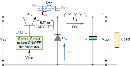
A buck switching regulator is a DC-DC converter and one of the simplest and most common types of switching regulators. When used in a switch-mode power supply configuration, a buck switching regulator uses a series transistor or a power MOSFET (which is an insulated gate bipolar transistor or IGBT) as its primary switching device, as shown below.
Buck Switching Regulator
We can see that the basic circuit configuration of a buck converter is a series transistor switch TR 1 with associated drive circuitry (to keep the output voltage as close to the desired level as possible), diode D 1, inductor L1 and smoothing capacitor C 1. The buck converter has two operating modes, depending on whether the switching transistor TR 1 is “on” or “off”.
When the transistor is biased “ON” (switch closed), diode D1 becomes reverse biased and the input voltage VIN causes current to flow through the inductor to the load connected at the output, charging capacitor C1.
As a varying current flows through the inductor coil, according to Faraday's law, it generates a back EMF which opposes the current flow until it reaches a steady state, creating a magnetic field around the inductor, L 1. This continues indefinitely as long as TR1 is closed.
When transistor TR1 is turned “off” (switch opened) by the control circuit, the input voltage is immediately disconnected from the emitter circuit, causing the magnetic field around the inductor to collapse, thus developing a reverse voltage across the inductor.
This reverse voltage causes the diode to become forward biased, so the energy stored in the inductor's magnetic field forces current to continue flowing in the same direction through the load and back through the diode.
Inductor L1 then returns its stored energy to the load, acting as a power source and supplying current until all of the inductor's energy is returned to the circuit or until the transistor switch is closed again, whichever comes first. At the same time, the capacitor also discharges, supplying current to the load. The combination of the inductor and capacitor forms an LC filter that smooths out any ripple created by the transistor switching action.
So when the transistor solid state switch is closed, the current is provided by the supply, and when the transistor switch is open, the current is provided by the inductor. Note that the current flowing through the inductor is always in the same direction, either directly from the supply or through the diode, but obviously at different times within the switching cycle.
Since the transistor switch is continuously closed and opened, the average output voltage value will be related to the duty cycle D, which is defined as the on-time of the transistor switch during one complete switching cycle.
If V IN is the supply voltage, and the “ON” and “OFF” times of the transistor switch are defined as: t ON and t OFF , then the output voltage V OUT is:

The duty cycle of the buck converter can also be defined as:

Buck Switching Regulator Duty Cycle
Therefore, the larger the duty cycle, the higher the average DC output voltage of the switching power supply. From this we can also see that since the duty cycle D can never reach 1 (unity), the output voltage will always be lower than the input voltage, resulting in a buck regulator.
Voltage regulation is achieved by varying the duty cycle, with switching speeds up to 200kHz, allowing the use of smaller components, thereby significantly reducing the size and weight of the switch mode power supply.
Another advantage of a buck converter is that the inductor-capacitor (LC) arrangement provides very good inductor current filtering. Ideally, a buck converter should be operated in continuous switching mode so that the inductor current never drops to zero. If ideal components were used, with zero voltage drop and switching losses in the "on" state, an ideal buck converter could have an efficiency of up to 100%.
In addition to the step-down switching regulator used in the basic design of a switch-mode power supply, there is another mode of operation of the basic switching regulator, which is a step-up regulator, known as a boost converter.
- The basic principles of power supply design. What are the key components of a power supply?
- Cleverly use the electronic ballast of waste energy-saving lamps as power supply transformer
- Fabrication of multi-cell lithium battery charging circuit
- Lithium battery overcharge, over discharge, short circuit protection circuit design
- Recommended circuits for different power on times of LM4911
- Driving circuit that controls LED brightness using PWM signal
- Simple and practical LED lamp driving circuit
- Parallel DC regulated power supply circuit diagram
- Homemade low-power UPS
- USB power socket using the car battery
- Power circuit of STR5412
- Solar power circuit
- Household emergency power circuit
- Power circuit for home appliance repair
- Wide input 350mA LED driver circuit based on NCL30000
- Neon light high voltage power supply circuit
- Common power circuits and applications 09
- Common power circuits and applications 03
- JFET-MOSFET headphone circuit diagram
- SI9114 uses MOSFET circuit diagram


 京公网安备 11010802033920号