How to judge the design quality of printed circuit boards?
Source: InternetPublisher:宋元浩 Keywords: Printed Circuit Board PCB Updated: 2025/02/18
During the PCB layout process, there are many traces, and the signals in some of the traces may be low-level, low-noise signals. According to the MCU development engineer, in this case, they must be removed from the chaotic PCB traces to avoid noise. Sometimes these traces may be fast data or clock signals, which are separated from many pins on the chip. In order to match the length of the traces and keep a short distance, delay mismatch can be avoided.
If these traces are not designed correctly, some PCBs may work fine, while others may simply not function, depending on the characteristics and tolerances of the components used to populate each PCB. In other words, even if the PCB implements the interconnection of all electronic components as per the schematic, the final product may not work as expected.
So, how do you judge the design quality of a printed circuit board (PCB)?
1. PCB routing
Take an overall look at the visible traces on the PCB. These will be covered in solder mask, a thin, lacquer-like layer of polymer that covers the copper traces to prevent oxidation and shorts. This layer is usually green, but other colors can be used. Note that white solder mask tends to make traces the hardest to see. In most cases, just use the standard green color.
Also, only the top and bottom layers are actually visible, and if the board has more than two layers, you won't be able to see the inner layers. Still, reviewing only the outer layers should provide some clues about the quality of the design.
First, see if all traces run in straight segments without sharp bends. Sharp angles can be troublesome for some high-power and high-frequency traces. Rather than trying to determine which traces can accept 90° bends, it is better to simply avoid them. In any case, most CAD
PCB layout software packages can avoid this problem.
Note that there are some exceptions. Some printed inductors are square concentric spirals, and some printed antennas have sharp bends as features. However, both of these are easy to identify.
2. Decoupling capacitors
All chips require power to function properly, but what happens when the power supply is some distance away from the chip that needs power? In these cases, power must be supplied to the chip via PCB traces (although usually through a PCB power plane on an inner layer).
Decoupling capacitors are placed very close to the power pins of the chip to filter out any high frequency noise, this is done to avoid negatively affecting the chip. Typically, if a chip has multiple VDD pins, each such pin requires at least one decoupling capacitor, and sometimes more.
These decoupling capacitors should be physically located very close to the pins they are supposed to decouple. If this does not happen, their effectiveness will be greatly reduced. If your PCB design does not place decoupling capacitors next to the power pins of most microchips, then this is not designed correctly.
3. Length balance of PCB traces
In designs that require precise timing relationships between multiple signals, the lengths of PCB traces must be matched. This is important, for example, when routing high-speed clock signals to multiple chips or when running data and address buses between a microprocessor and RAM memory.
This ensures that all signals arrive at their destination with the same delay, preserving the relationship between the signal edges. This requires looking at the schematic and knowing which groups of signal lines require a precise timing relationship.
Then, follow the traces to see if some kind of trace length equalization (called a delay line) has been implemented.
Be aware that vias in signal paths can cause additional delays. If these issues cannot be avoided, check all traces that require a precise timing relationship and make sure they have the same number of vias. Alternatively, you can use delay lines to compensate for the delays caused by vias.
4. Antenna Feeder
If your design includes a radio transmitter, receiver, or transceiver (a transmitter and receiver combined), it must have an antenna. For best performance, the feed line between the radio frequency (RF) pins on the RF chip should match the impedance of the feed line connected to it. In turn, this feed line must match the impedance of the antenna.
This impedance matching is necessary to maximize power transfer between the antenna and the radio chip. Any mismatch results in a reduction in the actual transmitted power, thus reducing the operating range. This feedline is simply a PCB trace with a controlled impedance that matches the antenna impedance (usually 50Ω).
If the output impedance of the transmitter does not match the impedance of the feed line, a matching network consisting of an inductor and a capacitor is usually employed. To achieve controlled impedance, the feed line is a PCB trace with a calculated width running over the ground plane. The width of this trace depends on the thickness of the copper trace, the thickness of the PCB substrate, and the dielectric constant.
If the antenna is a PCB antenna, it should be on one side of the PCB, without any ground plane. It should be clear of any other traces and away from any large components. Silkscreen markings around the antenna are usually fine, but copper markings (such as the PCB number or company name) can detune the antenna.
5. Component placement
In addition to placing decoupling capacitors, there are other considerations for placing components on the board:
If your circuit contains inductors, you should not place them too close together. Inductors generate magnetic fields. Placing them close together, especially end to end, can cause unwanted coupling between them.
Additionally, inductors should not be placed near large metal objects. The magnetic field can induce currents in these objects, which can change the value of the inductor.
Toroidal or donut-shaped inductors are generally less prone to generating stray magnetic fields, so their effects are less important. If it is unavoidable to place inductors close together, they should be placed perpendicular to each other to reduce unwanted mutual coupling.
If the board contains power resistors or any components that generate a lot of heat, you need to consider the effect of that heat on other nearby components. For example, if the circuit contains a thermistor to compensate for the effects of ambient temperature, it should not be placed near any power resistors. The same goes for temperature compensation capacitors.
If the circuit contains an on-board switching regulator, all components associated with it should be physically located on one part of the PCB and as far away as possible from the parts that handle small signals. These tend to generate significant switching noise that can negatively affect sensitive circuit parts.
If the PCB has AC power applied directly to the power section, the AC side should be located on one part of the circuit board.
Additionally, the PCB itself should have a physical barrier to separate the AC from the rest of the board. Typically, this is accomplished by having a slot in the PCB that separates the two sections.
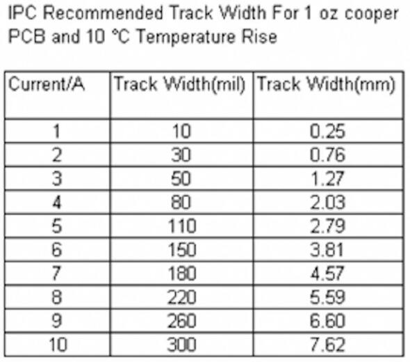
6. Trace Width and Routing
Traces carrying high currents should be sized appropriately. Figure 2 below shows the recommended trace widths for different current ratings:
Due to noise pickup issues, traces carrying small analog signals should not run parallel to traces carrying digital or fast-changing signals. Also, generally speaking, traces connecting inductors should not be wider than necessary. They may act like antennas and generate unwanted RF emissions.
7. Ground and Plane
For any moderately complex PCB, it is best to use at least a four-layer board, with the two inner layers being power and ground planes.
If the design contains both analog and digital sections, the ground planes should be separated and connected only at a common point (usually the negative supply). This prevents large ground current spikes from the digital section from adversely affecting the analog section.
If only two layers are used, each sub-circuit ground return trace should be separated and all these sub-paths should be connected to the negative power supply terminal. It is a bad design to have the ground return of any sub-section or IC go into the common ground return path and then back to the negative power supply terminal as shown in Figure 3 below.
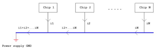
The problem here is that PCB copper traces do have some resistance. Therefore, current flowing through the trace will cause a voltage drop. In the example above, the chip on the far right of the trace will see its ground reference voltage as higher than the actual ground reference voltage. Furthermore, its ground will bounce based on the return current of all the chips on the left side of the diagram.
- Inverting Operational Amplifier Circuit Analysis
- TL783 parameters/pin configuration and functions, tl783 parameter circuit diagram
- Analysis of Operational Amplifier Differentiator Circuit
- This article will tell you the hard requirements of operational amplifiers
- Classification and characteristics of operational amplifiers, classification and characteristics of operational amplifiers
- What is the difference between CPLD and FPGA?
- How do you calculate the value of capacitors in series? Why use capacitors in series?
- DIY a decorative lamp
- Analysis of three simple electronic dice circuits
- Make a flameless electronic candle using simple electronics and LEDs
- Impedance control of through holes in PCB design and its impact on signal integrity
- How to design a switching power supply?
- Comparison between hard board PCB and soft board FPC
- PCB circuit board via hole plug hole overview
- PCB board interconnection method
- Crystal oscillator PCB design considerations
- How to connect the components in PCB?
- Some summaries of PCB wiring
- PCB schematic diagram reverse derivation step method
- PCB layout and routing rules analysis


 京公网安备 11010802033920号