Analysis of Operational Amplifier Differentiator Circuit
Source: InternetPublisher:吃掉星星 Keywords: Operational amplifier differential circuit Updated: 2025/02/18
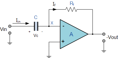
The differential amplifier, as the name implies, is a circuit that performs differential operations in an operational circuit. The MCU development engineer said that similar to the inverting amplifier, we swap the positions of the capacitor and the resistor, connecting the reactance XC to the input terminal of the inverting amplifier, and the resistor Rf forms a negative feedback element on the operational amplifier as usual. As shown below:
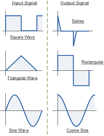
This op amp circuit performs the mathematical operation of differentiation, which means "producing an output voltage that is proportional to the rate of change of the input voltage with respect to time." In other words, the faster or larger the change in the input voltage signal, and the greater the input current, the greater the change in the output voltage in response, and the more "spike-like" the shape.
As with the integrator circuit, a resistor and a capacitor form an RC network across the op amp, and the reactance of the capacitor (Xc) plays an important role in the performance of the op amp differentiator.
Introduction to Operational Amplifier Differentiator Circuits
The input signal to the differentiator is applied to the capacitor. The capacitor blocks any DC component, so no current flows to the amplifier's summing point X, resulting in an output voltage of zero. The capacitor only allows changes in the AC input voltage to pass, with a frequency that depends on the rate of change of the input signal.
At low frequencies, the reactance of the capacitor is "high", resulting in low gain (Rf/Xc) and a low output voltage of the op amp. At higher frequencies, the reactance of the capacitor is much lower, resulting in higher gain and a higher output voltage of the differential amplifier.
However, at high frequencies, the differentiator circuit of the op amp becomes unstable and will start to oscillate. This is mainly due to first order effects, which determine the frequency response of the op amp circuit, thus causing a second order response, which at high frequencies gives an output voltage much higher than expected. To avoid this, the high frequency gain of the circuit needs to be reduced by adding an additional small capacitor across the feedback resistor Rf.
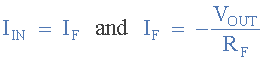
Since the op amp has a zero node voltage at its inverting input, the current I flowing through the capacitor will be given as:
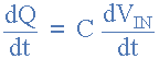
The charge on a capacitor is equal to the capacitance multiplied by the voltage across the capacitor:

Therefore, the rate of change of this fee is:
But DQ/dt is the capacitor current, I:
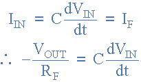
From this we can conclude that the ideal voltage output of the op amp differentiator is:
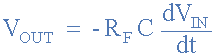
Therefore, the output voltage Vout is the constant –Rf*C times the derivative of the input voltage Vin with respect to time. The negative sign (–) indicates a phase shift of 180° because the input signal is connected to the inverting input terminal of the operational amplifier.
As a final point to mention, the op amp differentiator circuit in its basic form has two major disadvantages compared to the previous op amp integrator circuit. One is that it suffers from instability at high frequencies as mentioned above, and the other is that the capacitive input makes it very susceptible to random noise signals, and any noise or harmonics present in the source circuit will be amplified more than the input signal itself. This is because the output is proportional to the slope of the input voltage, so some method of limiting the bandwidth is required to achieve closed loop stability.
Operational Amplifier Differentiator Waveforms
If we apply a continuously varying signal (such as a square, triangle or sine wave type signal) to the input of a differential amplifier circuit, the resulting output signal will vary, with its final shape depending on the RC time constant of the resistor/capacitor combination.
The basic single resistor and single capacitor op amp differentiator circuit is not widely used to reform the mathematical function of differentiation due to the two inherent errors mentioned above ("instability" and "noise"). Therefore, in order to reduce the overall closed-loop gain of the circuit at high frequencies, an additional resistor, Rin, is added to the input as shown below.
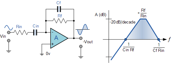
Adding input resistor R IN limits the gain of the differentiator to the ratio of R f / R IN . The circuit now behaves like a differentiator amplifier at low frequencies and like an amplifier with resistive feedback at high frequencies, providing better noise rejection.
Additional attenuation of higher frequencies can be achieved by connecting a capacitor Cf in parallel with the differentiator feedback resistor Rf. This forms the basis of an active high pass filter as we have seen previously in the filter section.
- What is a touch sensor? How does a touch sensor work?
- Understanding the capacitance formula, what are the types of capacitors
- Summary of I2C basics: How does I2C communication actually work?
- LM337 pin diagram and parameters, LM337 application circuit diagram
- What is a photocoupler and how to select and use one?
- What is a pure resistance circuit? What is a pure resistance AC circuit?
- What is an ac to dc transformer in circuit design
- How to identify common mode interference? Methods to eliminate common mode interference
- DIY a decorative lamp
- Beautiful crown wreath made with LED
- AC ammeter
- High Stability Thermocouple Amplifier
- Practical amplifier circuit g composed of operational amplifier LM386
- Practical amplifier circuit b composed of operational amplifier LM386
- Practical amplifier circuit b composed of operational amplifier LM386
- Operational amplifier output circuit
- High input impedance buffer amplifier circuit
- Alarm circuit of a typical electromagnetic stove
- Interface circuit between thyristor and operational amplifier
- Simple clock signal circuit consisting of a single operational amplifier


 京公网安备 11010802033920号