How to Build a TIA Circuit Using a Fully Differential Amplifier
Source: InternetPublisher:3228 Keywords: Differential transimpedance amplifier Updated: 2025/08/19
Transimpedance amplifiers (TIAs) are most commonly constructed using operational amplifiers (op amps). Furthermore, an increasing number (if not all) of analog-to-digital converters (ADCs) are fully differential systems, requiring a single-ended differential mechanism. Due to their high bandwidth, TIAs are commonly used in high-speed circuits, such as those in optical transmission and communication systems. For example, a PIN-TIA optical receiver is a detection device used in optical communication systems to convert weak optical signals into electrical signals and amplify them with a certain level of intensity and low noise. Its operating principle is as follows: when the PIN's photosensitive surface is illuminated by detection light, the pn junction is reverse-biased, causing photogenerated carriers to drift under the influence of the electric field, generating a photocurrent in the external circuit. This photocurrent is amplified and output by a transimpedance amplifier, thus achieving the conversion of the optical signal into an electrical signal and subsequent initial amplification. In practical applications, depending on the TIA's requirements, a -5.2 V, 3.3 V, or other power supply scheme is used, along with various peripheral circuitry to complete the package.
As we know, in DWDM systems, OSNR (Signal-to-Noise Ratio) is a key indicator of overall system transmission performance. It's the ratio of signal to noise. To improve the signal-to-noise ratio to an ideal transmission performance value, the above description demonstrates the use of a TIA, which amplifies electrical signals with a certain level of intensity and low noise. After optical fiber transmission, signals inevitably experience some attenuation due to optical power and dispersion. When an optical amplifier converts the optical signal into an electrical signal for amplification, the TIA effectively suppresses the amplification of the noise signal, reducing the denominator and increasing the numerator. This makes it easy to understand how the TIA improves the optical signal-to-noise ratio (OSNR). Simply put, under the same conditions, it's a technical device used to minimize negative factors and maximize positive factors.
For applications requiring DC coupling, this is primarily accomplished by using a fully differential amplifier (FDA).
Is there a way to use FDA for I-to-V conversion and interface directly with an ADC? The short answer is yes, and here we will review the implementation and limitations.
Before proceeding further, I need to warn you about using an FDA as a gain limiter for a TIA. The input bias current of a bipolar input stage effectively limits the maximum achievable gain of the transimpedance stage. You can expect input bias currents of several microamperes. In an op amp, if both the input bias current and the feedback resistor are large, this will cause an offset at the output. In an FDA, the input bias current will cause a common-mode offset. This isn't a problem, as the output voltage swing is twice that of an op amp with an FDA output stage, but it needs to be considered for higher transimpedance gains.
Let's start with the OPA843, a bipolar amplifier with excellent noise and gain-bandwidth. Set to a gain of 20kW and using a 1.5pF input capacitor with the photodiode, the OPA843 achieves a flat frequency response of approximately 57MHz under these conditions. See Figure 1 below.
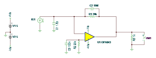
Figure 1: OPA843 TIA configuration
The properties of interest that we will monitor are:
1- Small signal frequency response and its associated flatness to ensure the absence of ringing in the impulse response and well-behaved phase variations.
2- Integrated noise at the output.
3- Power consumption of the solution.
Figures 2 and 3 show the performance of the OPA843 monitored here.
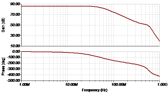
Figure 2: OPA843 frequency response
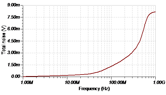
Figure 3: OPA843 integrated output noise
The OPA843 consumes approximately 200mW when operating on ±5V supplies.
Looking at the 14mA on the +5V supply FDA (70mW) THS4520, we can achieve the same 20kΩ transimpedance gain by using a 10kΩ resistor in the feedback path. C4 is required to achieve this gain of 20kΩ. Note that for frequencies below the pole formed by R2 and C4 (here, 16Hz), the gain is reduced by 6dB.
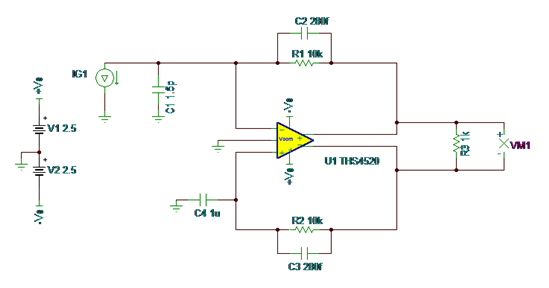
Figure 4: THS4520 TIA configuration
Despite the increased bandwidth, the THS4520 achieves approximately 74MHz of bandwidth with significantly lower integrated noise than the OPA843. This reduced noise is due in part to the THS4520's lower current noise density (for the same voltage noise density), but also due to the lower noise gain resulting from the lower feedback resistor and higher compensation feedback capacitor used to achieve the same gain. The two main terms contributing to the noise reduction are lower noise gain vs. frequency and lower feedback resistor and its associated thermal noise. The results are plotted in Figures 5 and 6.
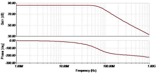
Figure 5: THS4520 frequency response
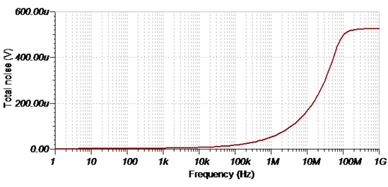
Figure 6: THS4520 integrated output noise
Three key factors determine the bandwidth of a TIA:
1 Total input capacitance (CTOT).
2 The ideal transimpedance gain is set by RF.
3. Gain-Bandwidth Product (GBP) of the operational amplifier: A higher gain-bandwidth produces a higher closed-loop transimpedance bandwidth.
These three factors are interrelated: for a particular op amp, positioning the gain sets the maximum bandwidth; conversely, positioning the bandwidth sets the maximum gain.
When designing a TIA, it is important to understand the capacitance of the photodiode, as this capacitance is typically determined by the application. Given the photodiode capacitance, the next step is to select an amplifier that is appropriate for the application.
Selecting the appropriate amplifier requires understanding the relationship between the amplifier's GBP, the desired transimpedance gain and closed-loop bandwidth, and the input and feedback capacitances.
- 300W LM3886 Power Amplifier
- RS-485 Receiver Basics
- Transistor circuit diagram explanation
- Four constant current source circuits and their applications in integrated operational amplifier circuits
- How to use an amplifier to build a high current pulse source
- How to Build a TIA Circuit Using a Fully Differential Amplifier
- Correcting DC Errors in High-Speed Amplifier Circuits
- Using diodes to make a capacitor charging and discharging experimental circuit
- Some Techniques for Calculating Transistor Amplifier Circuits
- Detailed explanation of hysteresis comparator circuit diagram and transfer characteristics
- Essentials of making a tube amplifier
- Valuables detection circuit design
- High-end four-channel mixer
- Circuit diagram of a thermocouple cold junction temperature compensation
- Op amp impedance multiplication circuit
- Variable gain operational amplifier circuit diagram
- Adjustable output voltage regulator circuit diagram
- Ultrasonic proximity sensor circuit
- non-diode rectifier
- Infrared remote control transmitter/receiver circuit


 京公网安备 11010802033920号