Transistor circuit diagram explanation
Source: InternetPublisher:aytwartoofyoroo Keywords: triode Updated: 2025/09/16
Figure 1 shows a common-emitter circuit for an NPN transistor. Figure 2 shows its characteristic curve, which shows three operating regions: the cutoff region, the linear region, and the saturation region. The transistor uses the B-pole current, IB, as input to control the transistor's operating state. If the transistor is in the cutoff region, IB approaches 0 (VBE also approaches 0), the C-pole and E-pole are essentially open-circuited, IC = 0, and VCE = VCC. If the transistor is in the linear region, the BE junction is forward biased and the BC junction is reverse biased. The value of IB is moderate (VBE = 0.7 V), and IC = hFE. IB is proportionally amplified, with VCE = Vcc - Rc. IB can be controlled by IB. If the transistor is in the saturation region, IB is very large, VBE = 0.8 V, VCE = 0.2 V, and VBC = 0.6 V. Both the BC and BE junctions are forward biased, and the junctions between CE and CE are equivalent to a path with a 0.2 V potential drop. Therefore, Ic = (Vcc - 0.2)/Rc. Ic is independent of IB. Since IB at this point is greater than the IB value in the linear amplification region, Ic < hFE IB is inevitable. In the cutoff state, the junctions between CE and CE act as an open circuit. In the saturation state, the junctions between CE and CE act as a path (with a 0.2 V potential drop), thus functioning as a switch. This switch is controlled by IB, and VBB can also be used as the control input signal. Figures 3 and 4 show the open and closed states of a transistor switch, respectively, and their corresponding equivalent circuits.
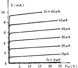
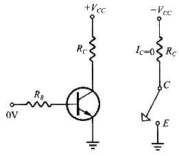
Figure 1 NPN transistor common emitter circuit Figure 2 Common emitter circuit output characteristic curve
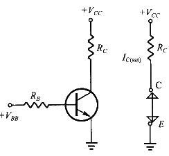
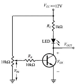
Figure 3: Cutoff state is like a disconnected circuit. Figure 4: Saturated state is like a connected circuit.
Experiment: The switching function of a transistor
is simple. Transistor switch: The circuit is shown in Figure 5. Resistor RC is the LED current limiter to prevent excessive voltage from burning out the LED (light-emitting diode). Adjust the input signal VIN from 0 to maximum (divided into approximately 20 equal steps). Observe and record the corresponding VOUT and LED brightness. When the transistor switch is off, VOUT = VCC = 12 V, and the LED does not light. When the transistor switch is on, VOUT = 0.2 V, and the LED lights up. Improved transistor switch: Because a transistor transitions from the cutoff region to the saturation region through the linear region, the switching effect does not have a clear boundary. To make the switching effect more clear, two transistors can be connected in series. The circuit is shown in Figure 6. Similarly, adjust the input signal VIN from 0 to maximum (divided into approximately 20 equal steps). Observe and record the corresponding VOUT and LED brightness.
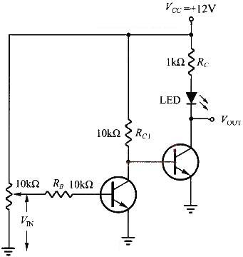
Figure 5: Simple switching transistor circuit diagram.
As can be seen above, almost any transistor type can be used as an electronic switch, and if conditions permit, it can also be used to control heating equipment. While the term "switching transistor" is a general concept, a few specialized switching transistors are available on the market.
- 12V lamp current indicator
- MC34063 circuit calculation formula and application explanation
- Circuit model of an ideal transformer
- Connecting It Up: High-Speed LVDS Comparators
- Introduction to Photosensitive Devices
- Principle of multiplier voltage rectifier circuit
- Using diodes to make a capacitor charging and discharging experimental circuit
- Single voltage comparator circuit diagram
- Gate resistor and bleeder resistor
- Detailed explanation of hysteresis comparator circuit diagram and transfer characteristics
- Detailed explanation of the working principle of linear regulated power supply
- Color changing flash light principle circuit diagram
- Improved connection method of triode switch circuit circuit diagram
- Circuit diagram of triode inverter
- Composite pipe a
- Single supply complementary symmetrical circuit
- Improved multivibrator circuit a
- 24V, 500mA regulated power supply circuit
- Precision regulated power supply circuit for UJ-1 type potentiometer
- One of the boiling water alarm circuits


 京公网安备 11010802033920号