Design a 100A active load to test power supply reliability
Source: InternetPublisher:公子李 Keywords: Active load power supply test Updated: 2025/08/22
We use an active load test circuit to ensure that the power supply to a microprocessor or other digital load can deliver 100A transient current. This active load presents a DC load to the power supply and can rapidly switch between DC levels. These transient loads simulate the fast logic switching in the microprocessor.
Ideally, your regulator output is constant during load transients. However, in practice, you'll encounter some variation, which can be problematic if the permitted operating voltage tolerance is exceeded. You can base your active load circuit on a previous broadband load design that operates at lower currents. This approach allows you to design a closed-loop, 500kHz bandwidth, 100A active load with a linear response.
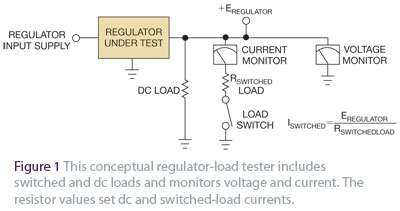
Traditional active load circuits have drawbacks (Figure 1). The regulator under test drives a DC and switched resistive load. The switch current and output voltage are monitored to compare the stable output voltage versus load current under static and dynamic conditions. The switch current is either on or off. When it changes, you cannot control it in the linear region.
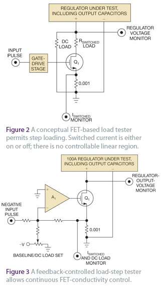
You can further develop this concept by including electronic load switching control (Figure 2). The input pulse switches the FETs through the driver stage, generating a transient load current from the regulator and its output capacitors. The size, composition, and placement of these capacitors have a profound impact on transient response. While electronic control facilitates high-speed switching, this architecture cannot simulate loads between minimum and maximum currents. Furthermore, you don't control the switching speed of the FETs, as doing so would introduce broadband harmonics into the measurement, which could corrupt the oscilloscope display.
transient generator
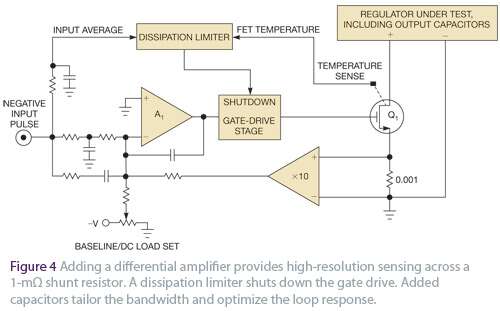
Placing Q1 in the feedback loop enables true linear control of the load tester (Figure 3). You can now linearly control Q1's gate voltage, allowing you to set the instantaneous transient current at any point and simulate nearly any load curve. Feedback from Q1's source to control amplifier A1 closes the control loop around Q1, stabilizing its operating point. The instantaneous input control voltage and the value of the current-sense resistor set Q1's current over a wide bandwidth. You use the DC load-setting potentiometer to bias A1 to Q1's conduction threshold. Small changes in A1's output result in large changes in Q1's current, meaning A1 doesn't need to provide large output excursions. The fundamental speed limitation is the amplifier's small-signal bandwidth. As long as the input signal remains within this bandwidth, Q1's current waveform is identical to A1's input control voltage waveform, enabling linear control of the load current. This versatile capability allows you to simulate a wide variety of loads.
You can improve this circuit by adding a few components (Figure 4). The gate-drive stage isolates the control amplifier from Q1's gate capacitance to maintain the amplifier's phase margin and provide low latency and linear current gain. A difference amplifier with a gain of 10 provides high-resolution sensing across the 1mΩ shunt resistor. You can design a power limiter that acts on the average input value and Q1's temperature. It shuts down the FET's gate drive to prevent overheating and subsequent damage. Capacitors can be added to the main amplifier to adjust the bandwidth and optimize the loop response.
Based on these concepts, you can develop a detailed schematic (Figure 5). The main amplifier, A1, responds to both DC and pulsed inputs. It also receives a feedback signal from A3, which represents the load current. A1 sets Q1's conductivity via the Q4/Q5 gate-drive stage, which is actively biased using A2. The voltage drop across the gate-driver input diodes will be high enough to fully turn on Q4 and Q5. To prevent this overdrive, use Q3 to reduce the voltage across the lower diode. Amplifier A2 determines the gate-drive stage bias by comparing Q5's average collector current to a reference value and controlling the conduction of Q3, thereby closing the loop. This loop maintains the voltage drop across the bases of Q4 and Q5 well below 1.2V, servoing this value until Q4 and Q5 have an average collector bias current of 10mA.
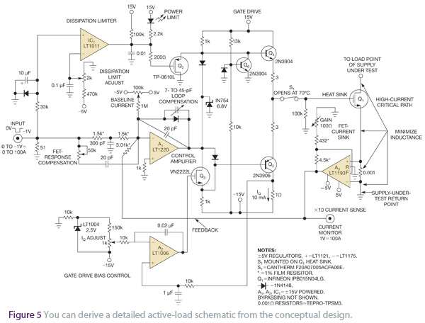
If the load is on for too long, the load's duty cycle can overheat. You can design a protection circuit using techniques used by designers of high-power pulse generators. Comparator IC 1 is fed the average input voltage value. It compares this voltage to a reference voltage set using the dissipation limit adjustment potentiometer. If the input duty cycle exceeds this limit, comparator IC 1 shuts off the FET gate drive through Q 2. Thermal switch S 1 provides further protection. If Q 1's heat sink overheats, S 1 opens and disconnects the gate drive signal. By diverting the bias voltage of Q 4, transistor Q 6, and the Zener diode, Q 1 is prevented from turning on when the -15V supply is absent. A 1-kΩ resistor on the positive input of A 1 prevents damage to the amplifier if the 15V supply is lost.
Trimming optimizes dynamic response, determines the loop's DC baseline idle current, sets dissipation limits, and controls the gate driver stage bias. DC trimming is self-explanatory. AC trimming of loop compensation and FET response at A1 is more subtle. Adjust them to obtain the best compromise between loop stability, edge rate, and pulse purity. You can use A1's loop compensation trimming capacitor to set the roll-off for maximum bandwidth and accommodate the phase shift introduced by Q1's gate capacitance and A3. FET response adjustment partially compensates for Q1's inherent nonlinear gain characteristic, improving the angular fidelity of preceding and following pulses.
Circuit testing
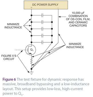
You initially tested the circuit using a fixture equipped with generous, low-loss, broadband bypassing (Figure 6). It's crucial to use a very low-inductance layout in the high-current path. Every effort must be made to minimize the inductance in the 100A path. If you minimize the inductance in the high-current path (Figure 7), you should achieve good results after properly tuning the circuit. The high-speed waveform with a 100A amplitude is pure, with virtually no visible inconsistencies in the top and bottom corners.
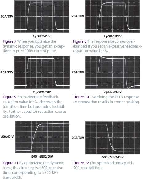
To investigate the effects of AC trimming on the waveform, you must intentionally mis-adjust. An overdamped response is typical of excessive A1 feedback capacitance (Figure 8). The current pulse is well controlled, but the edge rate is slow. Insufficient A1 feedback capacitance shortens transition time but increases instability (Figure 9). Further reducing the trimming capacitance results in loop oscillation, as the loop's phase shift causes a significant phase lag in the feedback. A scope photo of the uncontrolled 100A loop oscillation was not obtained. The event was too dramatic to record. Excessive FET response compensation results in peaking at the waveform corners (Figure 10). Restoring the AC trim to nominal value yields a 650 nanosecond rise time on the leading edge, equivalent to a 540 kHz bandwidth (Figure 11). Examining the trailing edge under the same conditions reveals a slightly faster fall time of 500 nanoseconds (Figure 12).
Layout Effect
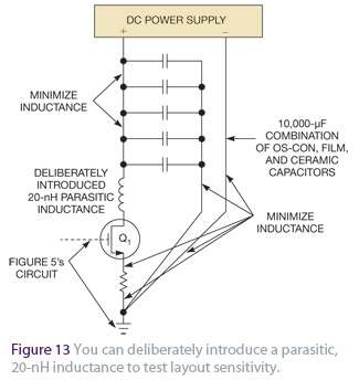
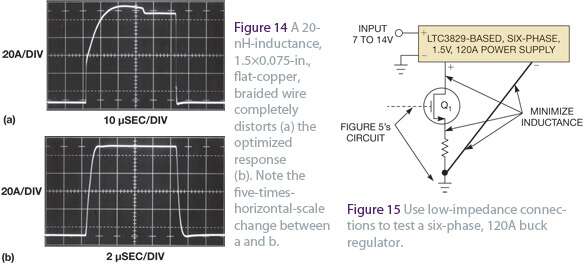
If parasitic inductance is present in the high-current path, your design won't even come close to matching the previous response. You can intentionally place a tiny 20nH parasitic inductance in Q1's drain path (Figure 13), which will result in significant waveform degradation caused by the inductance and subsequent response of the loop (Figure 14a). A significant error dominates the leading edge before recovery occurs midway through the top of the pulse. Additional distortion is evident during the falling turn-off. The horizontal scale of this graph is five times slower than the optimized response (Figure 14b). The lesson is clear: high-speed 100A excursions cannot tolerate inductance.
Regulator test
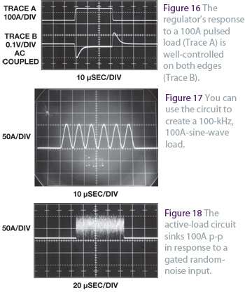
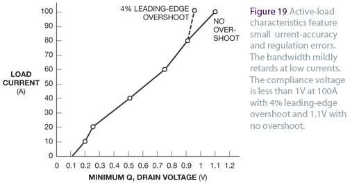
After addressing compensation and layout issues, you can test the power regulator (Figure 15). A six-phase, 120A Linear Technology LTC1675A buck regulator serves as a demonstration board. The test circuit generates a 100A load pulse (Trace A in Figure 16). The regulator maintains good control response at both edges (Trace B in Figure 16). The active load's true linear response and high bandwidth allow for a wide range of load waveform characteristics. While the step load pulse in Figure 16 is a commonly required test, you can generate any load profile. A 100A, 100kHz sine wave pulse train is an example (Figure 17). Despite the high speed and current, the response is clean, with no undesirable dynamics. Even an 80µs burst of 100A pp noise can be formed into the load (Figure 18). The load circuit exhibits high accuracy, compliance, and regulation specifications (Figure 19 and Table 1).
- 0-30V Mini Desktop Power Supply
- 12V dual power supply
- Dual-channel adjustable power supply
- Vehicle-mounted 12V to 50V DC converter
- Lithium-ion battery charger
- 12V to ±30V DC-DC converter
- Introduction to inverter circuit and principle
- Tips on how to optimize voltage monitors
- Top Three Ways to Split Voltage Rails into Bipolar Power Supplies
- When debugging a boost converter, you can analyze it from four directions.
- Three-way DC-DC converter circuit
- 2-phase CPU power circuit using HIP6301 and HIP6601 chips
- Head amplifier dedicated power supply circuit
- DC power supply circuit for semiconductor radio
- Antenna amplifier synchronous power supply circuit
- Music power circuit
- Neon light high voltage power supply circuit
- Common power circuits and applications 05
- ±5V, ±12V power circuit A
- Maintenance and experiment of multi-purpose power circuits


 京公网安备 11010802033920号