

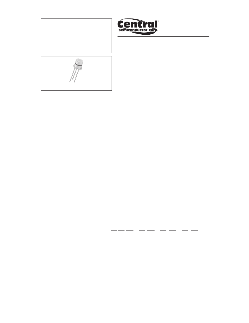
Small Signal Bipolar Transistor, 0.1A I(C), 32V V(BR)CEO, 1-Element, PNP, Silicon, TO-18,
| Parameter Name | Attribute value |
| Is it lead-free? | Lead free |
| Is it Rohs certified? | conform to |
| Maker | Central Semiconductor |
| package instruction | CYLINDRICAL, O-MBCY-W3 |
| Reach Compliance Code | compliant |
| ECCN code | EAR99 |
| Is Samacsys | N |
| Maximum collector current (IC) | 0.1 A |
| Collector-emitter maximum voltage | 32 V |
| Configuration | SINGLE |
| Minimum DC current gain (hFE) | 45 |
| JEDEC-95 code | TO-18 |
| JESD-30 code | O-MBCY-W3 |
| JESD-609 code | e3 |
| Number of components | 1 |
| Number of terminals | 3 |
| Maximum operating temperature | 200 °C |
| Package body material | METAL |
| Package shape | ROUND |
| Package form | CYLINDRICAL |
| Peak Reflow Temperature (Celsius) | 260 |
| Polarity/channel type | PNP |
| Certification status | Not Qualified |
| surface mount | NO |
| Terminal surface | MATTE TIN (315) |
| Terminal form | WIRE |
| Terminal location | BOTTOM |
| Maximum time at peak reflow temperature | 10 |
| transistor applications | SWITCHING |
| Transistor component materials | SILICON |
| Nominal transition frequency (fT) | 100 MHz |
| Maximum off time (toff) | 400 ns |
| Maximum opening time (tons) | 100 ns |
| Base Number Matches | 1 |
| BCY78-VIIILEADFREE | BCY78-XLEADFREE | BCY78-IXLEADFREE | BCY79-IXLEADFREE | BCY78-VIILEADFREE | BCY79-VIIILEADFREE | BCY79-VIILEADFREE | BCY79-XLEADFREE | |
|---|---|---|---|---|---|---|---|---|
| Description | Small Signal Bipolar Transistor, 0.1A I(C), 32V V(BR)CEO, 1-Element, PNP, Silicon, TO-18, | Small Signal Bipolar Transistor, 0.1A I(C), 32V V(BR)CEO, 1-Element, PNP, Silicon, TO-18, | Small Signal Bipolar Transistor, 0.1A I(C), 32V V(BR)CEO, 1-Element, PNP, Silicon, TO-18, | Small Signal Bipolar Transistor, 0.1A I(C), 45V V(BR)CEO, 1-Element, PNP, Silicon, TO-18, | Small Signal Bipolar Transistor, 0.1A I(C), 32V V(BR)CEO, 1-Element, PNP, Silicon, TO-18, | Small Signal Bipolar Transistor, 0.1A I(C), 45V V(BR)CEO, 1-Element, PNP, Silicon, TO-18, | Small Signal Bipolar Transistor, 0.1A I(C), 45V V(BR)CEO, 1-Element, PNP, Silicon, TO-18, | Small Signal Bipolar Transistor, 0.1A I(C), 45V V(BR)CEO, 1-Element, PNP, Silicon, TO-18, |
| Is it lead-free? | Lead free | Lead free | Lead free | Lead free | Lead free | Lead free | Lead free | Lead free |
| Is it Rohs certified? | conform to | conform to | conform to | conform to | conform to | conform to | conform to | conform to |
| Maker | Central Semiconductor | Central Semiconductor | Central Semiconductor | Central Semiconductor | Central Semiconductor | Central Semiconductor | Central Semiconductor | Central Semiconductor |
| package instruction | CYLINDRICAL, O-MBCY-W3 | CYLINDRICAL, O-MBCY-W3 | CYLINDRICAL, O-MBCY-W3 | CYLINDRICAL, O-MBCY-W3 | CYLINDRICAL, O-MBCY-W3 | CYLINDRICAL, O-MBCY-W3 | CYLINDRICAL, O-MBCY-W3 | CYLINDRICAL, O-MBCY-W3 |
| Reach Compliance Code | compliant | compliant | compliant | compliant | compliant | compliant | compliant | compliant |
| ECCN code | EAR99 | EAR99 | EAR99 | EAR99 | EAR99 | EAR99 | EAR99 | EAR99 |
| Maximum collector current (IC) | 0.1 A | 0.1 A | 0.1 A | 0.1 A | 0.1 A | 0.1 A | 0.1 A | 0.1 A |
| Collector-emitter maximum voltage | 32 V | 32 V | 32 V | 45 V | 32 V | 45 V | 45 V | 45 V |
| Configuration | SINGLE | SINGLE | SINGLE | SINGLE | SINGLE | SINGLE | SINGLE | SINGLE |
| Minimum DC current gain (hFE) | 45 | 60 | 60 | 60 | 40 | 45 | 40 | 60 |
| JEDEC-95 code | TO-18 | TO-18 | TO-18 | TO-18 | TO-18 | TO-18 | TO-18 | TO-18 |
| JESD-30 code | O-MBCY-W3 | O-MBCY-W3 | O-MBCY-W3 | O-MBCY-W3 | O-MBCY-W3 | O-MBCY-W3 | O-MBCY-W3 | O-MBCY-W3 |
| JESD-609 code | e3 | e3 | e3 | e3 | e3 | e3 | e3 | e3 |
| Number of components | 1 | 1 | 1 | 1 | 1 | 1 | 1 | 1 |
| Number of terminals | 3 | 3 | 3 | 3 | 3 | 3 | 3 | 3 |
| Maximum operating temperature | 200 °C | 200 °C | 200 °C | 200 °C | 200 °C | 200 °C | 200 °C | 200 °C |
| Package body material | METAL | METAL | METAL | METAL | METAL | METAL | METAL | METAL |
| Package shape | ROUND | ROUND | ROUND | ROUND | ROUND | ROUND | ROUND | ROUND |
| Package form | CYLINDRICAL | CYLINDRICAL | CYLINDRICAL | CYLINDRICAL | CYLINDRICAL | CYLINDRICAL | CYLINDRICAL | CYLINDRICAL |
| Peak Reflow Temperature (Celsius) | 260 | 260 | 260 | 260 | 260 | 260 | 260 | 260 |
| Polarity/channel type | PNP | PNP | PNP | PNP | PNP | PNP | PNP | PNP |
| Certification status | Not Qualified | Not Qualified | Not Qualified | Not Qualified | Not Qualified | Not Qualified | Not Qualified | Not Qualified |
| surface mount | NO | NO | NO | NO | NO | NO | NO | NO |
| Terminal surface | MATTE TIN (315) | MATTE TIN (315) | MATTE TIN (315) | MATTE TIN (315) | Matte Tin (Sn) | Matte Tin (Sn) | Matte Tin (Sn) | Matte Tin (Sn) |
| Terminal form | WIRE | WIRE | WIRE | WIRE | WIRE | WIRE | WIRE | WIRE |
| Terminal location | BOTTOM | BOTTOM | BOTTOM | BOTTOM | BOTTOM | BOTTOM | BOTTOM | BOTTOM |
| Maximum time at peak reflow temperature | 10 | 10 | 10 | 10 | 10 | 10 | 10 | 10 |
| transistor applications | SWITCHING | SWITCHING | SWITCHING | SWITCHING | SWITCHING | SWITCHING | SWITCHING | SWITCHING |
| Transistor component materials | SILICON | SILICON | SILICON | SILICON | SILICON | SILICON | SILICON | SILICON |
| Nominal transition frequency (fT) | 100 MHz | 100 MHz | 100 MHz | 100 MHz | 100 MHz | 100 MHz | 100 MHz | 100 MHz |
| Maximum off time (toff) | 400 ns | 400 ns | 400 ns | 400 ns | 400 ns | 400 ns | 400 ns | 400 ns |
| Maximum opening time (tons) | 100 ns | 100 ns | 100 ns | 100 ns | 100 ns | 100 ns | 100 ns | 100 ns |
 京公网安备 11010802033920号


