
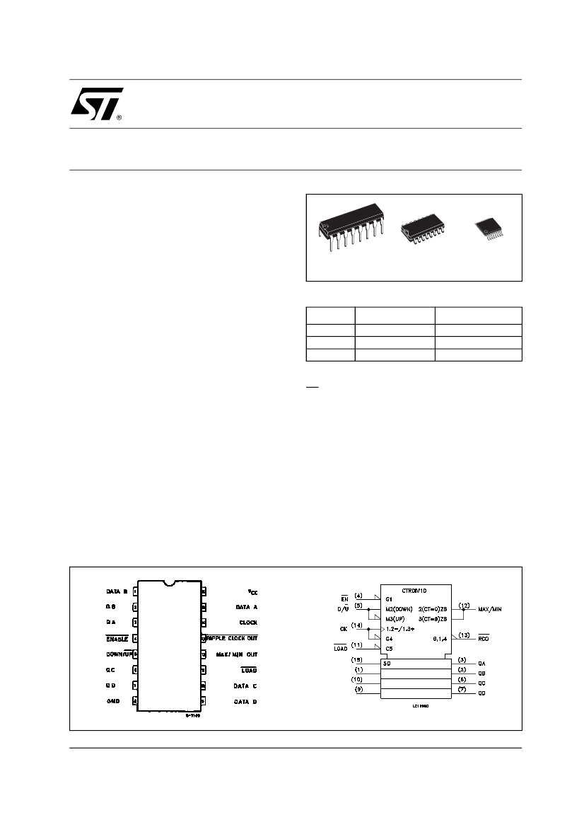
4 BIT SYNCHRONOUS UP/DOWN COUNTERS
| Parameter Name | Attribute value |
| Is it Rohs certified? | conform to |
| Maker | STMicroelectronics |
| Parts packaging code | SOIC |
| package instruction | SOP, SOP16,.25 |
| Contacts | 16 |
| Reach Compliance Code | compli |
| Other features | TCO OUTPUT |
| Counting direction | BIDIRECTIONAL |
| series | HC/UH |
| JESD-30 code | R-PDSO-G16 |
| JESD-609 code | e4 |
| length | 9.9 mm |
| Load capacitance (CL) | 50 pF |
| Load/preset input | YES |
| Logic integrated circuit type | DECADE COUNTER |
| Maximum Frequency@Nom-Su | 17000000 Hz |
| MaximumI(ol) | 0.004 A |
| Operating mode | SYNCHRONOUS |
| Number of digits | 4 |
| Number of functions | 1 |
| Number of terminals | 16 |
| Maximum operating temperature | 125 °C |
| Minimum operating temperature | -55 °C |
| Package body material | PLASTIC/EPOXY |
| encapsulated code | SOP |
| Encapsulate equivalent code | SOP16,.25 |
| Package shape | RECTANGULAR |
| Package form | SMALL OUTLINE |
| method of packing | TUBE |
| Peak Reflow Temperature (Celsius) | NOT SPECIFIED |
| power supply | 2/6 V |
| propagation delay (tpd) | 270 ns |
| Certification status | Not Qualified |
| Maximum seat height | 1.75 mm |
| Maximum supply voltage (Vsup) | 6 V |
| Minimum supply voltage (Vsup) | 2 V |
| Nominal supply voltage (Vsup) | 4.5 V |
| surface mount | YES |
| technology | CMOS |
| Temperature level | MILITARY |
| Terminal surface | Nickel/Palladium/Gold (Ni/Pd/Au) |
| Terminal form | GULL WING |
| Terminal pitch | 1.27 mm |
| Terminal location | DUAL |
| Maximum time at peak reflow temperature | NOT SPECIFIED |
| Trigger type | POSITIVE EDGE |
| width | 3.9 mm |
| minfmax | 20 MHz |
| M74HC190M1R | M74HC190_01 | M74HC190 | M74HC190B1R | M74HC190TTR | M74HC190RM13TR | |
|---|---|---|---|---|---|---|
| Description | 4 BIT SYNCHRONOUS UP/DOWN COUNTERS | 4 BIT SYNCHRONOUS UP/DOWN COUNTERS | 4 BIT SYNCHRONOUS UP/DOWN COUNTERS | 4 BIT SYNCHRONOUS UP/DOWN COUNTERS | 4 BIT SYNCHRONOUS UP/DOWN COUNTERS | 4 BIT SYNCHRONOUS UP/DOWN COUNTERS |
| Is it Rohs certified? | conform to | - | - | conform to | incompatible | conform to |
| Maker | STMicroelectronics | - | - | STMicroelectronics | STMicroelectronics | STMicroelectronics |
| Parts packaging code | SOIC | - | - | DIP | TSSOP | SOIC |
| package instruction | SOP, SOP16,.25 | - | - | DIP, DIP16,.3 | TSSOP, TSSOP16,.25 | SOP, SOP16,.25 |
| Contacts | 16 | - | - | 16 | 16 | 16 |
| Reach Compliance Code | compli | - | - | compli | _compli | compli |
| Other features | TCO OUTPUT | - | - | TCO OUTPUT | TCO OUTPUT | TCO OUTPUT |
| Counting direction | BIDIRECTIONAL | - | - | BIDIRECTIONAL | BIDIRECTIONAL | BIDIRECTIONAL |
| series | HC/UH | - | - | HC/UH | HC/UH | HC/UH |
| JESD-30 code | R-PDSO-G16 | - | - | R-PDIP-T16 | R-PDSO-G16 | R-PDSO-G16 |
| JESD-609 code | e4 | - | - | e3 | e0 | e4 |
| Load capacitance (CL) | 50 pF | - | - | 50 pF | 50 pF | 50 pF |
| Load/preset input | YES | - | - | YES | YES | YES |
| Logic integrated circuit type | DECADE COUNTER | - | - | DECADE COUNTER | DECADE COUNTER | DECADE COUNTER |
| Maximum Frequency@Nom-Su | 17000000 Hz | - | - | 17000000 Hz | 17000000 Hz | 17000000 Hz |
| MaximumI(ol) | 0.004 A | - | - | 0.004 A | 0.004 A | 0.004 A |
| Operating mode | SYNCHRONOUS | - | - | SYNCHRONOUS | SYNCHRONOUS | SYNCHRONOUS |
| Number of digits | 4 | - | - | 4 | 4 | 4 |
| Number of functions | 1 | - | - | 1 | 1 | 1 |
| Number of terminals | 16 | - | - | 16 | 16 | 16 |
| Maximum operating temperature | 125 °C | - | - | 125 °C | 125 °C | 125 °C |
| Minimum operating temperature | -55 °C | - | - | -55 °C | -55 °C | -55 °C |
| Package body material | PLASTIC/EPOXY | - | - | PLASTIC/EPOXY | PLASTIC/EPOXY | PLASTIC/EPOXY |
| encapsulated code | SOP | - | - | DIP | TSSOP | SOP |
| Encapsulate equivalent code | SOP16,.25 | - | - | DIP16,.3 | TSSOP16,.25 | SOP16,.25 |
| Package shape | RECTANGULAR | - | - | RECTANGULAR | RECTANGULAR | RECTANGULAR |
| Package form | SMALL OUTLINE | - | - | IN-LINE | SMALL OUTLINE, THIN PROFILE, SHRINK PITCH | SMALL OUTLINE |
| method of packing | TUBE | - | - | TUBE | TAPE AND REEL | TAPE AND REEL |
| Peak Reflow Temperature (Celsius) | NOT SPECIFIED | - | - | 245 | NOT SPECIFIED | NOT SPECIFIED |
| power supply | 2/6 V | - | - | 2/6 V | 2/6 V | 2/6 V |
| propagation delay (tpd) | 270 ns | - | - | 270 ns | 270 ns | 270 ns |
| Certification status | Not Qualified | - | - | Not Qualified | Not Qualified | Not Qualified |
| Maximum seat height | 1.75 mm | - | - | 5.1 mm | 1.2 mm | 1.75 mm |
| Maximum supply voltage (Vsup) | 6 V | - | - | 6 V | 6 V | 6 V |
| Minimum supply voltage (Vsup) | 2 V | - | - | 2 V | 2 V | 2 V |
| Nominal supply voltage (Vsup) | 4.5 V | - | - | 4.5 V | 4.5 V | 4.5 V |
| surface mount | YES | - | - | NO | YES | YES |
| technology | CMOS | - | - | CMOS | CMOS | CMOS |
| Temperature level | MILITARY | - | - | MILITARY | MILITARY | MILITARY |
| Terminal surface | Nickel/Palladium/Gold (Ni/Pd/Au) | - | - | Matte Tin (Sn) | Tin/Lead (Sn/Pb) | Nickel/Palladium/Gold (Ni/Pd/Au) |
| Terminal form | GULL WING | - | - | THROUGH-HOLE | GULL WING | GULL WING |
| Terminal pitch | 1.27 mm | - | - | 2.54 mm | 0.65 mm | 1.27 mm |
| Terminal location | DUAL | - | - | DUAL | DUAL | DUAL |
| Maximum time at peak reflow temperature | NOT SPECIFIED | - | - | NOT SPECIFIED | NOT SPECIFIED | NOT SPECIFIED |
| Trigger type | POSITIVE EDGE | - | - | POSITIVE EDGE | POSITIVE EDGE | POSITIVE EDGE |
| width | 3.9 mm | - | - | 7.62 mm | 4.4 mm | 3.9 mm |
| minfmax | 20 MHz | - | - | 20 MHz | 20 MHz | 20 MHz |
 京公网安备 11010802033920号


