
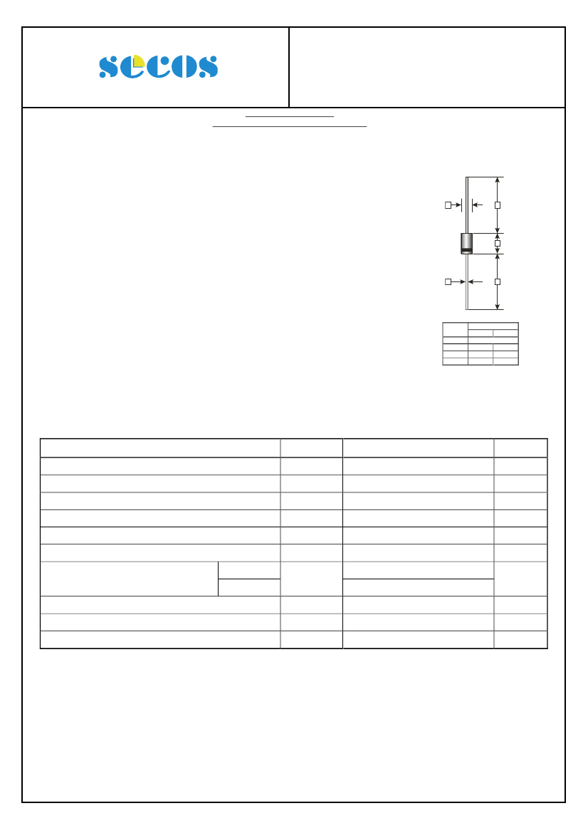
1 A, 200 V, SILICON, SIGNAL DIODE, DO-41
| Parameter Name | Attribute value |
| Is it Rohs certified? | conform to |
| Maker | SECOS |
| Parts packaging code | DO-41 |
| package instruction | O-PALF-W2 |
| Contacts | 2 |
| Reach Compliance Code | compli |
| ECCN code | EAR99 |
| Shell connection | ISOLATED |
| Configuration | SINGLE |
| Diode component materials | SILICON |
| Diode type | RECTIFIER DIODE |
| Maximum forward voltage (VF) | 0.9 V |
| JEDEC-95 code | DO-41 |
| JESD-30 code | O-PALF-W2 |
| JESD-609 code | e3 |
| Maximum non-repetitive peak forward current | 30 A |
| Number of components | 1 |
| Number of terminals | 2 |
| Maximum operating temperature | 150 °C |
| Minimum operating temperature | -55 °C |
| Maximum output current | 1 A |
| Package body material | PLASTIC/EPOXY |
| Package shape | ROUND |
| Package form | LONG FORM |
| Peak Reflow Temperature (Celsius) | NOT SPECIFIED |
| Maximum repetitive peak reverse voltage | 200 V |
| surface mount | NO |
| technology | SCHOTTKY |
| Terminal surface | Tin (Sn) |
| Terminal form | WIRE |
| Terminal location | AXIAL |
| Maximum time at peak reflow temperature | NOT SPECIFIED |
 京公网安备 11010802033920号


