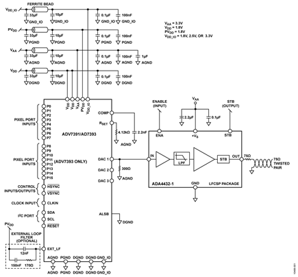
Circuit Function and Benefits The circuit in Figure 1 shows a digital-to-analog video converter paired with a low-cost, low-power, fully integrated reconstruction video filter with output short-to-battery (STB) protection, ideal for transmitting CVBS video in harsh infotainment environments such as automotive. Although many video encoders (video DACs) such as the ADV7391 can directly drive video loads, it is often beneficial to place a video driver at the output of the video encoder for power saving, filtering, line driving, and overvoltage circuit protection. The video driver is usually configured as an active filter (also called a reconstruction filter) and its main purpose is to block high-frequency components (above the Nyquist frequency) introduced into the video signal during the sampling process and to provide gain to drive the 750Ω external cable connected to the video display. Designers of infotainment and other video systems such as rearview cameras and rear-seat entertainment systems prefer this circuit to transmit video for the reasons mentioned above. However, there is a third pressing design issue, that of robustness. The ADA4432-1 and ADA4433-1 provide analog video designers with an integrated IC that features critical overvoltage protection, enhanced ESD tolerance, excellent video features, low power consumption, and line diagnostics. The ADA4432-1 and ADA4433-1 are fully integrated video reconstruction filters, single-ended and differential, respectively. They provide overvoltage protection up to 18 V at the output (STB protection), low power consumption, and line diagnostics. Line diagnostics are provided via logic outputs that can be activated when a fault condition occurs. The ADA4432-1 and ADA4433-1 include a high-order filter with a −3 dB cutoff frequency of 10 MHz and 45 dB rejection at 27 MHz. With STB protection and robust ESD tolerance, the ADA4432-1 and ADA4433-1 provide excellent protection in harsh environments. The ADV7391 and ADA4432-1 are fully qualified for automotive applications and are ideal for infotainment and visual safety systems in automotive applications. The ADV7391, ADA4432-1, and ADA4433-1 are available in very small LFCSP packages for small space applications. Circuit Description The ADV7391 is a low power, fully integrated digital video encoder that converts digital 8-bit component video data from a CMOS imager into standard analog baseband video signals compatible with worldwide standards. Three 10-bit digital-to-analog video converters (operating with VAA = 2.6 V to 3.46 V) support composite (CVBS), S-video (YC), or component (YPrPb/RGB) analog outputs in standard definition (SD) or high definition (HD) video formats. The circuit in Figure 1 is configured to provide low output drive through DAC1 only. To further reduce power consumption, the other DACs and phase-locked loop (PLL) are turned off. Low drive mode is defined by a 4.33 mA full-scale output current. The ADV7391 contains an RSET pin. A resistor is connected from the RSET pin to AGND to control the full-scale output current. For low drive operation, RSET must be equal to 4.12 kΩ and RL must be equal to 300 Ω. The resistor connected to the RSET pin must have a 1% tolerance. The ADV7391 contains an on-chip PLL that allows oversampling of the video data. As shown in Figure 1, the PLL is disabled (Subaddress 0x00, Bit 1 = 1), providing a 2× SD oversampling rate. With the PLL disabled, the external loop filter components are removed to save space and cost. The ADA4432-1 can be used as a pseudo-differential (single-ended) driver with an unbalanced transmission line. The pseudo-differential mode uses one conductor to carry the unbalanced data signal from the driver to the receiver and the other conductor as a ground reference signal. The positive conductor connects the ADA4432-1 output to the positive input of the differential receiver. The negative line or ground conductor from the source circuit is connected to the negative input of the receiver. The output termination resistors of the ADA4432-1 should match the impedance of the receiver input termination resistors. For example, in a 75Ω system, each output of the ADA4432-1 is back-terminated with 75Ω resistors that are connected to a 75Ω resistor at the receiver. In Figure 1, the ADA4432-1 is configured as a single-ended to single-ended driver, allowing unbalanced transmission using twisted pair, untwisted pair, or coaxial cable. Low Power Considerations Using the ADA4432-1 or ADA4433-1 with series source termination and shunt load termination at low supply voltages can achieve significant power savings compared to driving the video cable directly from the DAC output. Figure 2 shows a video DAC driving a cable directly. A properly terminated DAC driving the transmission line requires two 75Ω loads in parallel, requiring more than 33mA to achieve a full-scale voltage level of 1.3V. Figure 3 shows the same video load driven by the ADA4432-1 with series-shunt termination. This requires twice the output voltage to drive the equivalent 150Ω resistor, but only slightly more than 15 mA is required to achieve full-scale output. Using the same supply voltage as the DAC, this results in a 74% power savings compared to the circuit in Figure 2. The higher-order filtering provided by the ADA4432-1 reduces the DAC oversampling rate requirement, further reducing power consumption. The main source of power savings in the configuration shown in Figure 3 is the low drive mode setting of the ADV7391. Combined with the reduction in oversampling requirements (PLL off) and required load current, this mode can significantly reduce power consumption. For more information on low drive mode, refer to the ADV7391 data sheet. EMI and EMC Considerations The analog outputs of video DACs such as the ADV7391 require low-pass filtering to remove unwanted signal components with frequencies above the sampling rate or frequency sidebands. The conversion of digital-to-analog signals creates repeated images in the frequency domain at frequencies equal to multiples of the sampling frequency. The primary function of the reconstruction filter is to remove these frequency sideband components. This type of filter can significantly attenuate the sideband signals, thus preventing aliasing when decoding the DAC output. Aliasing errors can cause image quality issues. In addition, the image frequency sidebands can cause radiation in the output traces and lines, which can cause interference to adjacent circuits and other electronic systems. To reduce the impact of radiation, all unwanted high-frequency components should be removed before transmission along printed circuit board (PCB) traces and transmission cables. The ADA4432-1 can filter the DAC output and remove the unwanted high-frequency content, thereby helping to reduce EMI. Figures 4 to 6 illustrate this. Figure 4 shows the spectrum of a CVBS video signal at the output of the ADV7391 without the ADA4432-1. The spectrum shows a signal with a content bandwidth of 6.5 MHz, with sidebands at 27 MHz, 54 MHz, 108 MHz, and so on. The ADV7391 is operating in full output drive mode, with the PLL turned off and 2x oversampling. Figure 5 shows the spectrum of the same CVBS signal at the output of the ADA4332-1 without the ADV7391. The difference here is that while the ADV7391 is also operating in full output drive mode, the PLL is on and oversampling is performed by 8×. Figure 6 shows the spectrum of the same CVBS signal with the ADA4432-1 filtering the ADV7391 output. All sidebands are attenuated to less than 50 dB. The ADV7391 is operating in low output drive mode with the PLL off and oversampling by 2×. PCB Layout Considerations In any circuit where accuracy is important, careful consideration must be given to the layout of the power supply and ground return paths on the board. The digital and analog sections of the PCB should be isolated as much as possible. This PCB is constructed using a 4-layer stackup with large ground and power plane polygons. See the MT-031 Tutorial for a detailed discussion of layout and grounding and the MT-101 Tutorial for information on decoupling techniques. The power supplies to the ADV7391 are decoupled with 10 μF and 0.1 μF capacitors. Decouple the ADA4432-1 and ADA4433-1 output amplifiers with 0.1μF and 22μF capacitors to properly suppress noise and reduce ripple. These capacitors should be as close to the respective devices as possible, and the 0.1μF capacitors should have low ESR values. Ceramic capacitors are recommended for all high-frequency decoupling. It is important that the two ICs are as close to each other as possible. The power supply traces should be as wide as possible to provide a low impedance path and reduce the effects of glitches on the power supply line. Shield clocks and other fast switching digital signals from affecting other devices on the board through digital ground.
Blockdiagram


 京公网安备 11010802033920号

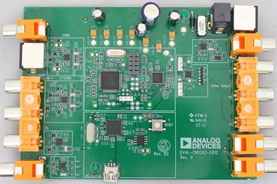
 CM2830ANIN92


