The circuit shown in Figure 1 uses the ADM3485E transceiver, a proven and tested electromagnetic compatibility (EMC) solution that provides triple protection for the widely used RS-485 communication port. Each solution is tested and characterized to ensure that the dynamic interactions between the transceiver and protection circuit elements work together to protect them from electrostatic discharge (ESD), electrical fast transients (EFT) and surges. Destruction - defined by IEC 61000-4-2, IEC 61000-4-4 and IEC 61000-4-5 standards respectively. This circuit uses the ADM3485E to provide proven ESD, EFT, and surge (common in harsh operating environments) protection for the RS-485 interface.


In industrial and instrumentation applications, the RS-485 bus standard is one of the most widely used physical layer bus design standards. RS-485 provides differential data transmission between multiple systems, which are often far apart. Applications for RS-485 include: process control networks, industrial automation, remote terminals, building automation (e.g., HVAC, security systems), motor control, and motion control.
In these real-world systems, lightning strikes, power surges, inductive switching, and electrostatic discharge can cause damage to communication ports by generating large transient voltages. Designers must ensure that the equipment will not only work under ideal conditions, but also in the harsh environments that it may actually encounter. To ensure that these designs can operate in electrically harsh environments, EMC regulations must be met.
Many EMC issues are not simple and easy to present, so they must be taken into account early in the product development cycle. Proper solutions and protection circuitry must be part of the overall design and not left to the last minute. The protection circuit must integrate the specific transceiver manufacturer's input and output structures as an integral part of the design.
The IEC 61000 specification defines a set of EMC immunity requirements. Within this set of specifications, designers must consider the following three types of high-voltage transients for data communications lines:
ESD and EFT have similar rise times, pulse widths and energy consumption levels. Surge transients have longer rise times and pulse widths; their amplitudes can ultimately be 3 to 4 orders of magnitude greater than those of ESD or EFT transients. Due to the similarities between ESD and EFT transients, their circuit protection designs are also similar. But because surge transients have higher energy levels, they must be treated differently.
Each solution provides ESD voltage (8 kV contact discharge and 15 kV air discharge) and 2 kV EFT voltage protection to the data port. Different solutions offer higher surge protection levels up to 6 kV. Circuit protection levels are listed in Table 1.
| protection plan |
ESD |
EFT( kV) | Surge(kV) |
| 1.TVS | Contact discharge: 8kV Air discharge: 15kV |
2 | 1 |
| 2.TVS/TBU/TISP | Contact discharge: 8kV Air discharge: 15kV |
2 | 4 |
| 3.TVS/TBU/GDT | Contact discharge: 8kV Air discharge: 15kV |
2 | 6 |
Figure 2 shows a physical photo of the EVAL-CN0313-SDPZ board. There are three ADM3485E devices on the board, one for each protection scheme. Each protection scheme provides the ESD and EFT protection described in this article and increases the level of surge protection.
For a complete design support package for the EVAL-CN0313-SDPZ board, including schematics, layout files, and bill of materials, see www.analog.com/CN0313-DesignSupport .

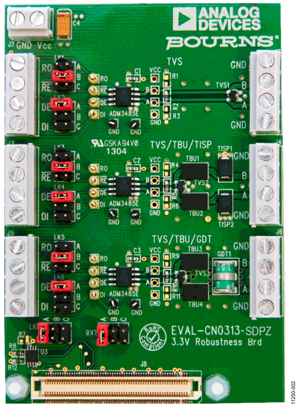
The ADM3485E is a 3.3 V low-power data transceiver suitable for half-duplex communications on multipoint transmission lines. It has data rates up to 12 Mbps and a common-mode voltage range of −7 V to +12 V on the bus pins (A and B). Data is sent out through the DI pin and received through the RO pin. The outputs of both the driver and receiver can be enabled or disabled into a high-impedance state by changing the corresponding logic levels on the DE and RE pins.
Power and ground are connected to each other (V CC . and GND) through spiral cable connectors that are used by all three ADM3485E devices.
The DE and RE logic inputs are set via LK1 to LK6. For each ADM3485E, LK2, LK4, and LK6 are related to DE; LK1, LK3, and LK5 are related to RE . related. For each link, position A connects the logic pin to V. Position B connects the logic pin to GND. Position C connects the logic pin to the four-pin side screw cable connector. The input DI and output RO pins connect directly to the four-pin screw connector.
EVAL-CN0313-SDPZ is also compatible with Analog Devices' ezLINX™ board ( EZLINX-IIDE-EBZ ) and system development platform ( EVAL-SDP-CB1Z ). Connector J8 connects the UART and GPIO interfaces on the SDP or ezLINX board to the logic I/O of the ADM3485E device. The I/O connections and jumper configurations are shown in Table 2.
| ADM3485E | I/O Pin |
SDP/ezLINX connector |
choose |
| TVS |
RO RE DE DI |
UART_RX GPIO_0 GPIO_3 UART_TX |
LK7(A) LK1(C) LK2(C) LK8(A) |
| TVS/TBU/TISP |
RO RE DE DI |
UART_RX GPIO_1 GPIO_4 UART_TX |
LK7(B) LK3(C) LK4(C) LK8(B) |
| TVS/TBU/GDT |
RO RE DE DI |
UART_RX GPIO_2 GPIO_5 UART_TX |
LK7(C) LK5(C) LK6(C) LK8(C) |
The ADM3485E transmitter and receiver share the same differential bus pins (A and B). Protection circuits are used to protect these bus pins.
In the first protection circuit (TVS, shown in Figure 1), a component is used, namely CDSOT23-SM712 from Bourns. It is a transient voltage suppressor (TVS) array on the EVALCN0313-SDPZ. It consists of two bidirectional TVS diodes optimized to protect RS-485 systems from as little overstress as possible while supporting the full range of RS-485 signals and common-mode voltage offsets. Under normal operating conditions, TVS has a high impedance to ground. When an overvoltage condition occurs, the TVS enters avalanche breakdown mode and clamps the pin voltage to a safe, predetermined level. It then diverts the transient current from the ADM3485E to ground.
This protection scheme provides up to 8 kV (contact discharge) and 15 kV (air discharge) ESD protection, 2 kV EFT protection and 1 kV surge protection.
As stated in the CDSOT23-SM712 data sheet, this device is designed for use with RS-485 devices. The following two protection schemes are applied to the CDSOT23-SM712 to provide more advanced circuit protection against surges.
In the second solution (TVS/TBU/TISP in Figure 1), the CDSOT23-SM712TVS provides the second level of protection, while Bourns' TISP4240M3BJR-S provides the first level of protection. TISP4240M3BJR-S is a fully integrated surge protector ( TISP ). TISP is a solid state thyristor. When its intended protection voltage is exceeded, the TISP provides a low-impedance path to ground, diverting most of the transient energy away from the ADM3485E.
Bourns' TBU-CA065-200-WH transient blocking unit ( TBU ) is a nonlinear overcurrent protection device located between the first and second level protection devices to ensure coordinated operation. TBU is an overcurrent blocking device that opens at a predetermined current. In blocking mode, it has a high impedance to block transient energy. This protection scheme provides up to 8 kV (contact discharge) and 15 kV (air discharge) ESD protection, 2 kV EFT protection and 4 kV surge protection.
The third level protection scheme ( TVS/TBU/GDT in Figure 1) works similarly to protection scheme 2. This scheme uses a gas discharge tube (GDT) instead of a TISP. The GDT protects against higher overvoltage and overvoltage conditions than the aforementioned TISP protection scheme. Current protection is provided. The GDT is a gas discharge plasma device that provides a low impedance ground path to prevent overvoltage transients. The selected GDT is Bourns' 2038-15-SM-RPLF.
This third level protection scheme provides up to 8 kV (contact discharge) and 15 kV (air discharge) ESD protection, 2 kV EFT protection and 6 kV surge protection.
The ADM3485E has a 120 Ω pin connected to the bus pin.


Blockdiagram
All reference designs on this site are sourced from major semiconductor manufacturers or collected online for learning and research. The copyright belongs to the semiconductor manufacturer or the original author. If you believe that the reference design of this site infringes upon your relevant rights and interests, please send us a rights notice. As a neutral platform service provider, we will take measures to delete the relevant content in accordance with relevant laws after receiving the relevant notice from the rights holder. Please send relevant notifications to email: bbs_service@eeworld.com.cn.
It is your responsibility to test the circuit yourself and determine its suitability for you. EEWorld will not be liable for direct, indirect, special, incidental, consequential or punitive damages arising from any cause or anything connected to any reference design used.
Supported by EEWorld Datasheet
EEWorld
subscription
account

EEWorld
service
account

Automotive
development
community

Robot
development
community

About Us Customer Service Contact Information Datasheet Sitemap LatestNews


Room 1530, 15th Floor, Building B,
No.18 Zhongguancun Street,
Haidian District,
Beijing, Postal Code: 100190
China
Telephone: 008610 8235 0740
 京公网安备 11010802033920号

 P6KE33C