The circuit shown in Figure 1 is a wideband receiver front end based on the ADL5562 ultra-low noise differential amplifier driver and the AD9467 16-bit, 250 MSPS analog-to-digital converter .
The third-order Butterworth anti-aliasing filter is optimized based on the performance and interface requirements of the amplifier and ADC. The total insertion loss caused by the filter network and other components is only 1.8 dB.
The overall 1 dB passband flatness of the circuit is 152 MHz. The measured SNR and SFDR at 120 MHz analog input are 72.6 dBFS and 82.2 dBc respectively.


This circuit accepts a single-ended input and converts it to differential form using a wide bandwidth (3 GHz) M/A-COM ECT1-1-13M 1:1 transformer. The 3.3 GHz differential amplifier ADL5562 has a differential input impedance of 400 Ω when operating at 6 dB gain and 200 Ω when operating at 12 dB gain. It also offers a 15.5 dB gain option.
The ADL5562 is an ideal driver for the AD9467. The fully differential architecture through the low-pass filter all the way to the ADC provides good high-frequency common-mode rejection and minimizes second-order distortion products. Depending on the input connection, the ADL5562 provides 6 dB or 12 dB of gain. This circuit uses 6 dB of gain to compensate for the insertion loss of the filter network and transformer (approximately 1.8 dB), resulting in a total signal gain of 3.9 dB.
An input signal of +6.0 dBm produces a 2 V pp full-scale differential signal at the ADC input.
The anti-aliasing filter is a third-order Butterworth filter designed using standard filter design programs. The Butterworth filter was chosen because it provides a flat response within the passband. The third-order filter produces an AC noise bandwidth ratio of 1.05 and can be designed with the help of several free filter programs, such as Nuhertz Technologies Filter Free (www.nuhertz/filter) or Quite Universal Circuit Simulator (Qucs) Free Simulation (www.qucs .sourceforge.net) etc.
For best performance, the ADL5562 should be loaded with a 200 Ω net differential load. The 15 Ω series resistor isolates the filter capacitor from the amplifier output, and the 243 Ω resistor in parallel with the downstream impedance, plus the 30 Ω series resistor, results in a net load impedance of 203 Ω.
A 20 Ω resistor in series with the ADC input isolates the internal switching transients from the filter and amplifier. The 511 Ω resistor in parallel with the ADC is used to lower the input impedance of the ADC, making its performance more predictable. The design parameters of the third-order Butterworth filter are as follows: source impedance 38.6 Ω, load impedance 269 Ω, and 3 dB bandwidth of 180 MHz. The values calculated by the program are shown in Figure 1. The filter passive component values chosen are the standard values that are closest to the values calculated by the program.

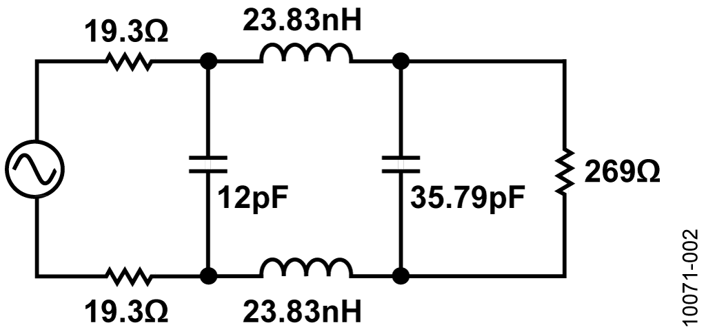
The value of the second parallel capacitor is subtracted from the ADC's 3.5 pF internal capacitance, resulting in a value of 32.29 pF. In this circuit, this capacitance is implemented using two 62 pF capacitors connected to ground, as shown in Figure 1. This achieves the same filtering effect and provides some AC common mode rejection.
System performance measurements are summarized in Table 1 with a 3 dB bandwidth of 152 MHz. The total insertion loss of this network is approximately 2 dB. The bandwidth response is shown in Figure 3, and the SNR and SFDR performance are shown in Figure 4.


Filter and interface design program
This section explains the general approach to amplifier/ADC and filter interface design. In order to achieve optimal performance (bandwidth, SNR, SFDR, etc.), there are some design limitations of the amplifier and ADC that must be considered for this general circuit:
The generalized circuit shown in Figure 5 is applicable to most high-speed differential amplifier/ADC interfaces and will be used as the basis for the discussion. This design approach often minimizes the filter's insertion loss by taking advantage of the relatively high input impedance of most high-speed ADCs and the relatively low impedance of the driving source (amplifier).
The basic design process is as follows:
After completing the above preliminary calculations, a quick check of the following items of the circuit should be made.
In some cases, a filter design program may provide more than one solution, especially for higher-order filters. At this time, a solution with the most reasonable combination of component values should be selected. Additionally, the chosen configuration should end with a shunt capacitor that can be combined with the ADC input capacitance.
Circuit Optimization Techniques and Tradeoffs
The parameters of this interface circuit interact with each other, so it is almost impossible to optimize all critical characteristics of the circuit (bandwidth, bandwidth flatness, SNR, SFDR, gain, etc.). However, by varying RA and RKB , the peaking that typically occurs in the bandwidth response can be minimized.
Notice in Figure 6 how the passband peaking decreases as the value of the output series resistor RA increases . However, the higher the value of this resistor, the greater the signal attenuation, and the amplifier must drive a larger signal to fill the ADC's full-scale input range.
The value of RA also affects SNR performance. Larger values on the one hand reduce bandwidth peaking, but on the other hand tend to slightly increase SNR because the signal level required to drive the ADC full scale is higher.
The series resistor R KB at the ADC input should be chosen to minimize distortion caused by any residual charge injection into the ADC's internal sampling capacitor. Increasing this resistance also tends to reduce bandwidth peaking.
However, increasing R KB increases the signal attenuation, and the amplifier must drive a larger signal to fill the ADC's input range. Another way to optimize passband flatness is to slightly change the filter shunt capacitance CAAF2 .
The ADC input termination resistor R TADC should generally be selected so that the ADC net input impedance is between 200 Ω and 400 Ω. Lowering its value will reduce the effect of the ADC input capacitance and may make the filter design more stable, but the downside is that it will increase the insertion loss of the circuit. Increasing its value also reduces peaking.


Striking a balance between these factors can be difficult. This design treats each parameter equally, so the values selected represent the interface performance for all design features. In some designs, different values may be chosen to optimize SFDR, SNR, or input drive levels, depending on system requirements.
The SFDR performance of this design depends on two factors: the amplifier and ADC interface component values shown in Figure 1, and the AD9467’s internal front-end buffer bias current setting through internal registers. The final SFDR performance numbers shown in Table 1 and Figure 4 were obtained after optimizing the SFDR as described in the AD9467 data sheet.
Another factor that can be weighed in this particular design is the ADC full-scale setting. For the data obtained with this design (optimized for SFDR), the ADC full-scale differential input voltage was set to 2 V pp. Moving the full-scale input range to 2.5 V pp improves SNR performance by approximately 1.5 dB but slightly reduces SFDR performance. The input range is set by the value loaded into the AD9467 internal registers, see the data sheet for details.
Note that the signal in this design is ac-coupled through a 0.1 μF capacitor to suppress the common-mode voltage between the amplifier, its termination resistor, and the ADC input. For more information on common-mode voltage, see the AD9467 data sheet.
Passive Components and PCB Parasitics Considerations
The performance of this or any high-speed circuit is highly dependent on proper PCB layout, including but not limited to power supply bypassing, controlled impedance traces (if required), component placement, signal routing, and power and ground planes. For PCB layout details for high-speed ADCs and amplifiers, see tutorials MT-031 and MT-101 .
Passive components in the filter should use low-parasitics surface-mount capacitors, inductors, and resistors. The inductor selected is Coilcraft 0603CS series. The surface mount capacitor used in the filter is 5%, C0G, 0402 type to ensure stability and accuracy.
For complete documentation on this system, see the CN-0227 Design Support Package ( www.analog.com/CN0227-DesignSupport ).


Blockdiagram
All reference designs on this site are sourced from major semiconductor manufacturers or collected online for learning and research. The copyright belongs to the semiconductor manufacturer or the original author. If you believe that the reference design of this site infringes upon your relevant rights and interests, please send us a rights notice. As a neutral platform service provider, we will take measures to delete the relevant content in accordance with relevant laws after receiving the relevant notice from the rights holder. Please send relevant notifications to email: bbs_service@eeworld.com.cn.
It is your responsibility to test the circuit yourself and determine its suitability for you. EEWorld will not be liable for direct, indirect, special, incidental, consequential or punitive damages arising from any cause or anything connected to any reference design used.
Supported by EEWorld Datasheet
EEWorld
subscription
account

EEWorld
service
account

Automotive
development
community

Robot
development
community

About Us Customer Service Contact Information Datasheet Sitemap LatestNews


Room 1530, 15th Floor, Building B,
No.18 Zhongguancun Street,
Haidian District,
Beijing, Postal Code: 100190
China
Telephone: 008610 8235 0740
 京公网安备 11010802033920号

 17H282105


