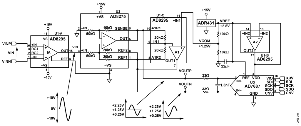
The circuit shown in Figure 1 is a complete analog front end that utilizes a 16-bit differential input PulSAR® ADC to digitally convert ±10 V industrial-grade signals. This circuit uses only two analog components to provide a high-impedance instrumentation amplifier input, level translation, attenuation, and differential conversion with high common-mode rejection (CMR) performance. Due to its high level of integration, this circuit saves printed circuit board space and provides a cost-effective solution for common industrial applications.
In process control and industrial automation systems, typical signal levels are up to ±10 V. Signal inputs from sensors such as thermocouples and load cells are smaller and therefore often encounter large common-mode voltage swings, which requires flexible analog inputs that can handle large and small differential signals with high common-mode rejection. Also has high impedance input.

When processing industrial-grade signals with modern low-voltage ADCs, attenuation and level conversion are necessary. In addition, fully differential input ADCs offer the following advantages: good common-mode rejection, fewer second-order distortion products, and a simplified DC adjustment algorithm. Therefore, industrial signals require further conditioning to interface correctly with differential input ADCs.
The circuit shown in Figure 1 is a complete and highly integrated analog front-end industrial-grade signal conditioner that uses only two active devices to drive the differential input 16-bit PulSAR ADC AD7687 : precision instrumentation amplifier (two auxiliary operations are integrated on-chip amplifier) AD8295 precision in-amp (with two on-chip auxiliary op amps) and AD8275 level converter/ADC driver . The ADR431, a low-noise 2.5V XFET® voltage reference, provides the reference voltage for the ADC.
The AD8295 is a precision instrumentation amplifier that integrates two non-dedicated signal processing amplifiers and two precision matched 20 kΩ resistors on-chip, and is packaged in a 4 mm × 4 mm package.
The AD8275 is a G = 0.2 differential amplifier that can be used to attenuate ±10 V industrial signals. The attenuated signal can be easily interfaced with a single-supply low-voltage ADC. The AD8275 performs the attenuation and level shifting functions in this circuit, maintaining good CMR without any external components.
The AD7687 is a 16-bit successive approximation ADC that operates from a single 2.3 V to 5.5 V supply. It uses differential inputs, has good CMR, and simplifies the use of SAR ADCs.
The circuit consists of the AD8295 and AD8275 used as analog front-end circuits, the ADC AD7687, and the reference voltage source ADR431, requiring only a few external components for decoupling, etc.
Instrumentation amplifier (integrated into AD8295)
The instrumentation amplifier (IA) integrated in the AD8295 is configured for a gain of 1. If the application requires higher gain, an appropriate external gain resistor can be added. The AD8295 supplies ±15 V and fully supports ±10 V industrial input signal levels. The reference pin of the instrumentation amplifier is connected to ground, so the output of the AD8295 is referenced to ground.
Differential Amplifier/Attenuator (AD8275)
The AD8295 instrumentation amplifier outputs a single-ended signal with a maximum amplitude of ±10 V. This signal must be attenuated and converted to the appropriate level to drive the AD7687 ADC. If you use a simple resistive level attenuator stage directly at the output of the AD8295, you will not be able to provide a differential output to drive the ADC. The AD8275 (G = 0.2) level translator is a difference amplifier with precision laser-trimmed matched thin film resistors ensuring low gain error, low gain drift (1 ppm/°C maximum), and high common-mode rejection (80 dB) characteristic. The AD8275 has a wide supply voltage range of +3.3 V to +15 V and a wide input voltage range of −12.3 V to +12 V when operating from a single +5 V supply.
The circuit shown in Figure 1 uses a balanced difference amplifier consisting of the AD8275 (U2) and a non-dedicated op amp from the AD8295 (U1-C). This op amp (U1-C) is used to invert the positive output of the AD8275 (thereby providing a complementary negative output) and drive the REF1 and REF2 pins of the AD8275. The output common-mode voltage for the differential output (VCOM = 1.25 V) is generated by an external 10 kΩ resistor divider connected to the 2.5 V reference and applied to the non-inverting input of U1-C. The equation describing the operation of the circuit is as follows:
VOUTP + VOUTN = 2 × VCOM
VOUTP = VOUTN + 0.2 × VIN
VOUTP = VCOM + 0.1 × VIN
VOUTN = VCOM − 0.1 × VIN
According to the above equation, for a ±10 V input voltage, each input voltage of the ADC (VOPTP and VOUTN) swings from 0.25 V to 2.25 V, 180° out of phase with each other, and has a common-mode voltage of 1.25 V. Therefore, the differential signal uses 4 V of the 5 V available differential input range of the ADC.
The ADR431 is a 2.5 V XFET family voltage reference that features low noise, high accuracy, and low temperature drift. The ADR431 drives the resistor divider and the reference voltage input of the AD7687 ADC. The ADR431 output is buffered by another non-dedicated op amp (U1-B) in the AD8295 and drives the AD7687 supply (VDD). A single-pole RC filter consisting of two 33 Ω resistors and a 1.5 nF capacitor serves as the 3 MHz cutoff antialiasing and noise reduction filter for the AD7687.
Layout and routing considerations
The performance of this or any high-speed/high-resolution circuit is highly dependent on proper PCB layout, including but not limited to power supply bypassing, signal routing, and proper power and ground planes. For details on PCB layout, see Tutorial MT-031 , MT-101 , and the article "A Practical Guide to High-Speed Printed Circuit Board Layout."


System performance
AC performance is tested at the system level with the AD7687 sampling at 250 kSPS. Figure 2 shows the FFT test results at 5 V pp 20 kHz input. Figure 3 shows the ADC output histogram with a 10 V DC input.
The evaluation software produced the following results:


Blockdiagram
All reference designs on this site are sourced from major semiconductor manufacturers or collected online for learning and research. The copyright belongs to the semiconductor manufacturer or the original author. If you believe that the reference design of this site infringes upon your relevant rights and interests, please send us a rights notice. As a neutral platform service provider, we will take measures to delete the relevant content in accordance with relevant laws after receiving the relevant notice from the rights holder. Please send relevant notifications to email: bbs_service@eeworld.com.cn.
It is your responsibility to test the circuit yourself and determine its suitability for you. EEWorld will not be liable for direct, indirect, special, incidental, consequential or punitive damages arising from any cause or anything connected to any reference design used.
Supported by EEWorld Datasheet
EEWorld
subscription
account

EEWorld
service
account

Automotive
development
community

Robot
development
community

About Us Customer Service Contact Information Datasheet Sitemap LatestNews


Room 1530, 15th Floor, Building B,
No.18 Zhongguancun Street,
Haidian District,
Beijing, Postal Code: 100190
China
Telephone: 008610 8235 0740
 京公网安备 11010802033920号

 25BSP11-Q-3-6