Background: When debugging serial communication in a project, serial communication tools are needed, sometimes TTL, sometimes RS232, and sometimes RS485. Using separate communication tools inevitably involves plugging and unplugging devices, which is cumbersome.
Sometimes a project uses both TTL and RS485, requiring multiple USB ports. Some computers (laptops) already have limited USB ports, and with numerous cables, this becomes even more inconvenient.
Three-in-one tools are available online, but they are expensive and only offer single-channel functionality.
This design uses the CH344, which has four serial ports. This perfectly solves the above problems, providing a three-in-one function: converting one USB interface to four serial ports, adding RS485 and RS232 circuitry,
and having pins for automatic RS485 transmission and reception, eliminating the need for a separate RS485 automatic transmission and reception circuit.
single-channel function: No switch is needed to achieve USB to TTL, USB to RS232, and USB to RS485 simultaneously.
When connecting the communication device to a computer and opening a serial port assistant, data will be sent from the TTL, RS232, and RS485 interfaces,
realizing three interfaces on a single serial port.
In addition to the communication interface, the communication device also has 5V and 3.3V power interfaces.
Voltage and current meters, power meters, and coulomb meters based on CW32f030 and ina226 schemes


Hardware Introduction:
Power Supply:
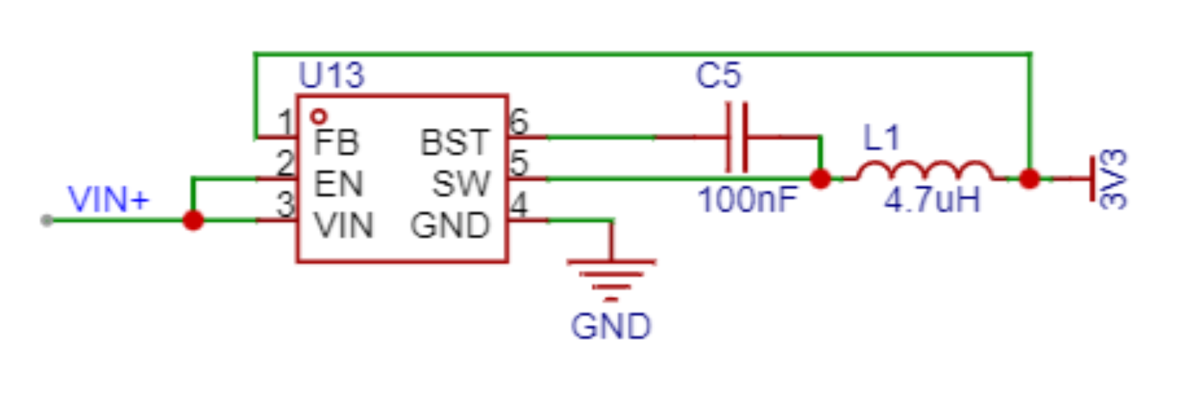
An AP63203 DC-DC converter is used, with a fixed 3.3V output. However, this power supply design had a slight mishap. The AP63203 DC-DC datasheet states a 3.3V output, but the actual output is about 0.1-0.3V higher, causing the ST7735 screen to display incorrectly when the input voltage is high. Fortunately, the solution is simple: short-circuit the 3.3V and 5V on the development board. Testing showed that after short-circuiting, the output was 3.4V with a 20V input, but this did not affect operation.

Note: After short-circuiting, never use the development board's built-in Type-C
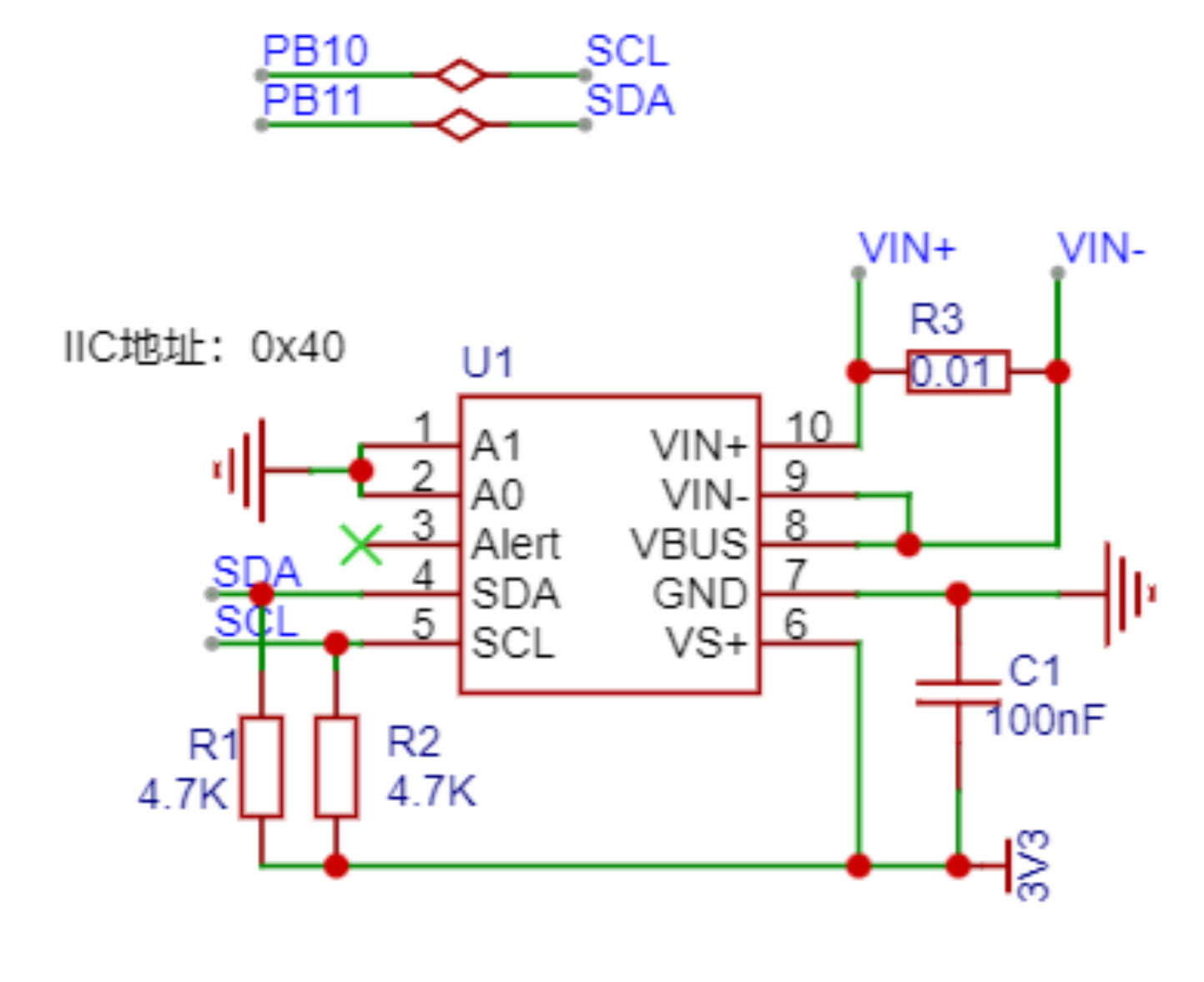
power supply. Voltage and Current Sampling:
TI's INA226 is used for sampling. It has a built-in 16-bit ADC, built-in op-amps, and can automatically average. It uses an IIC to connect to the host. The communication
main control MCU
is the LCSC-Diwenxing development board, built using the CW32F030C8T6 from Wuhan Xinyuan Semiconductor and a LCSC development board.
It's worth mentioning that the CW32F030C8T6 boasts a 32Mbits SPI refresh rate of 0.96, handling a 160*80 resolution screen with virtually no issues, significantly faster than the STM32F103's SPI. Thanks to the CW32F030C8T6's wide voltage range, it can operate normally even with slight power supply design issues. Additionally, the CW32F030C8T6 includes an advanced timer. Four general-purpose timers and three basic timers perfectly meet the requirements of this project

. The display screen
is a 0.96-inch, 160*80 resolution IPS display, communicating with the MCU via an SPI interface; this screen is very common

. Software components:
Overall software block diagram:
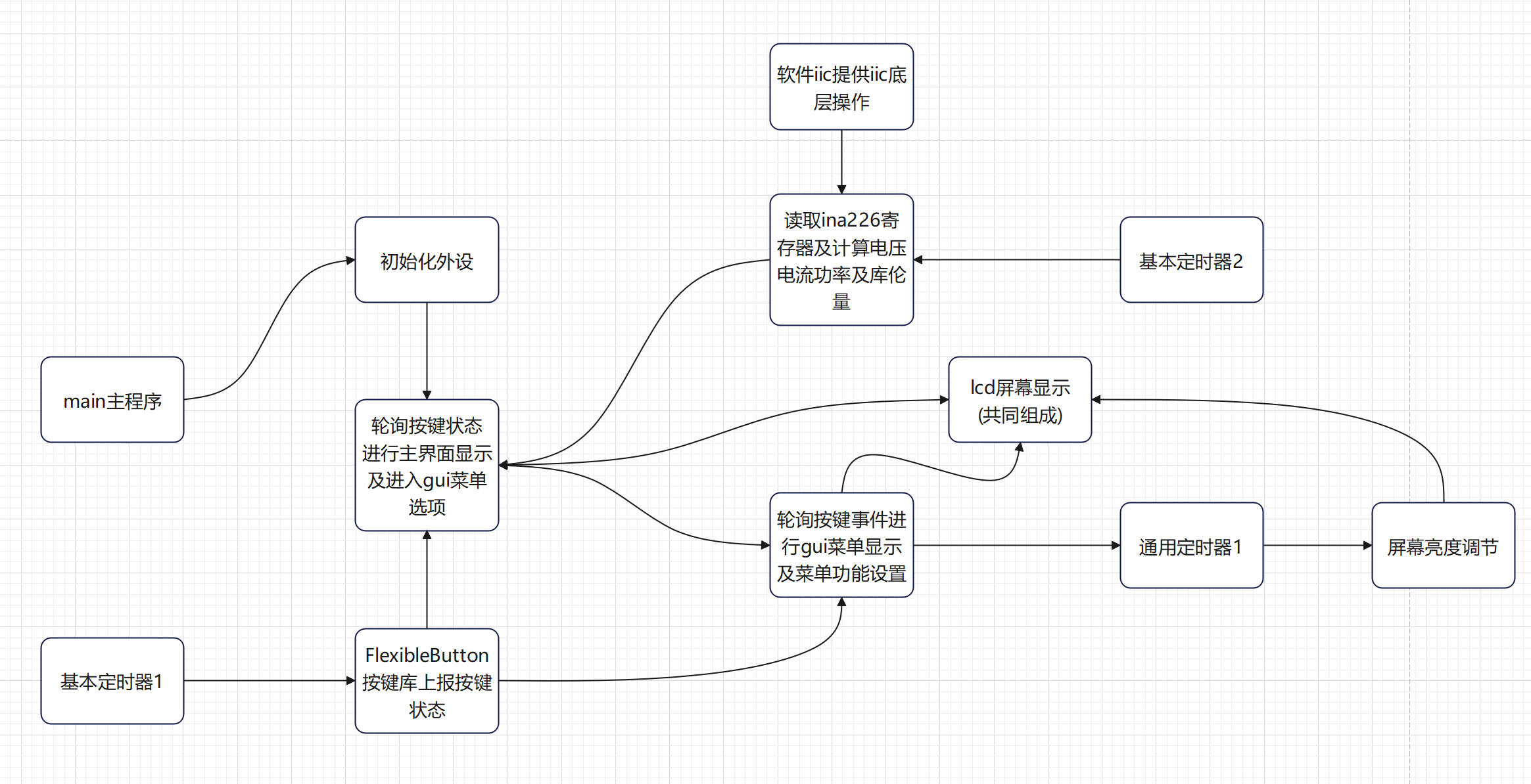
See source code: https://gitee.com/xmqor/cw32f030-mini-usb-voltage-ammeter
Function introduction:
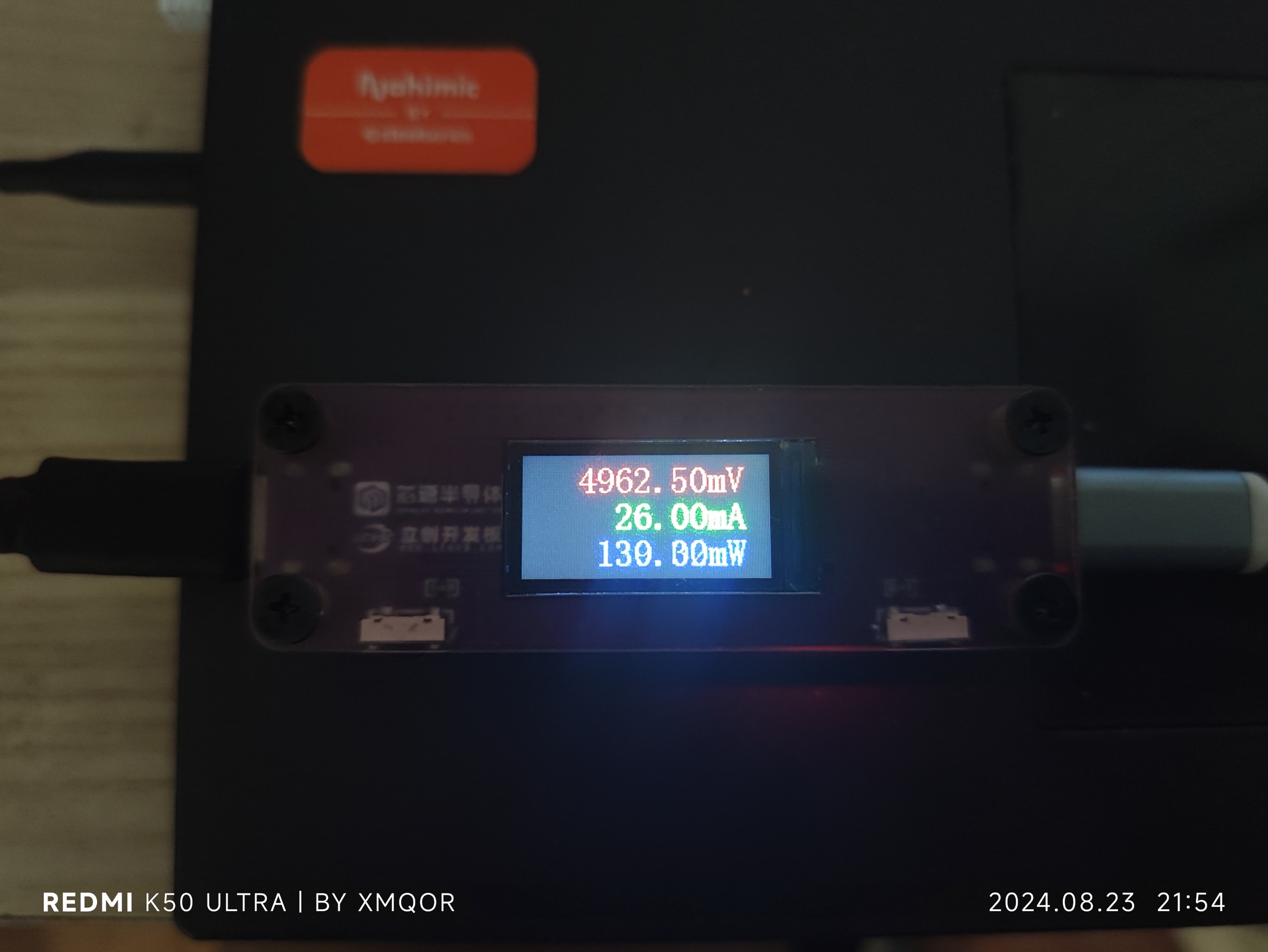
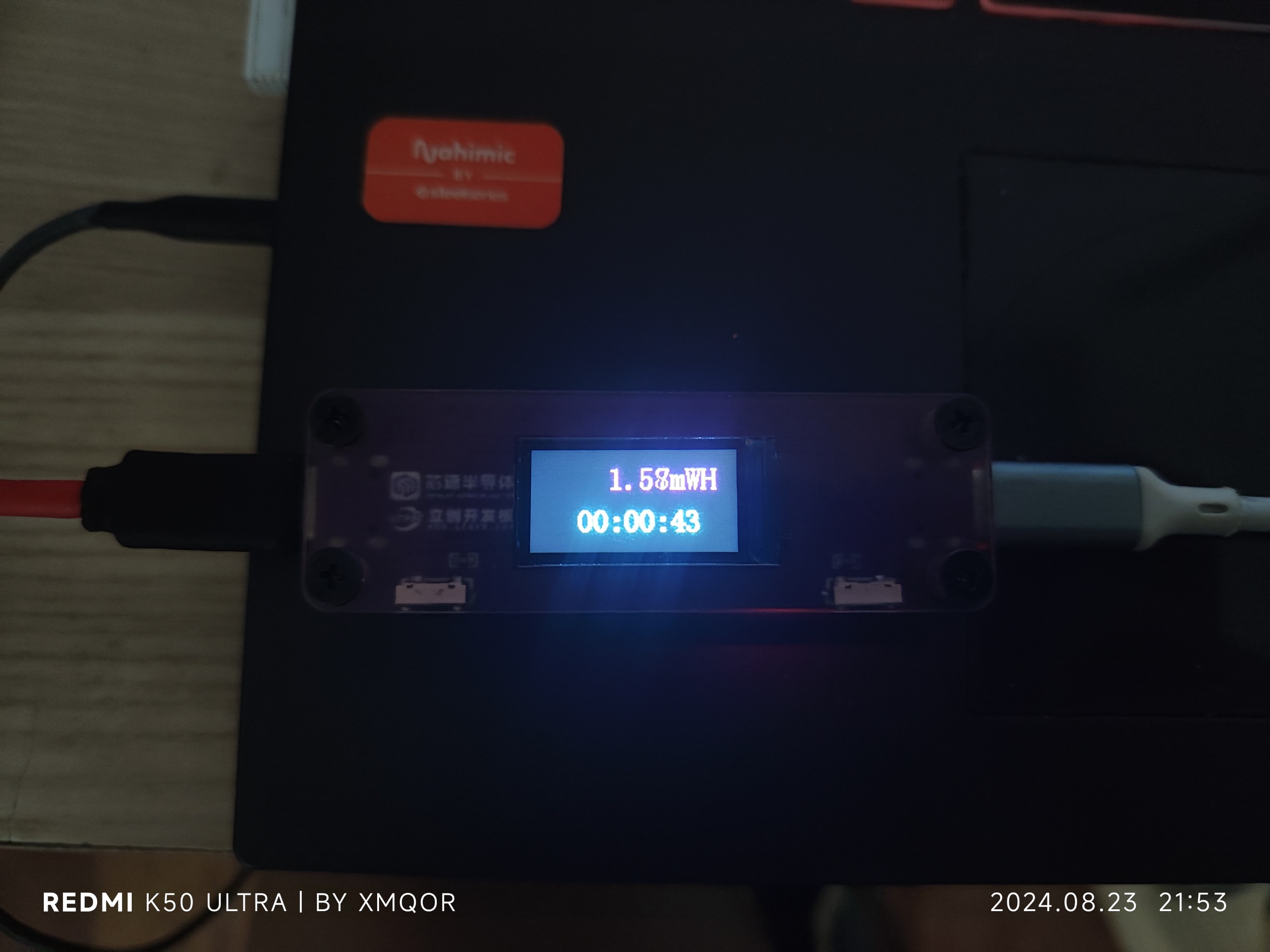
Voltage and current display: Resolution 0.25mV, 0.25mA, power is the product of voltage and current.
Coulomb meter: The coulomb meter samples power 100 times per second via a timer and calculates the integral.
UI menu:

UI operation instructions:
Main interface:
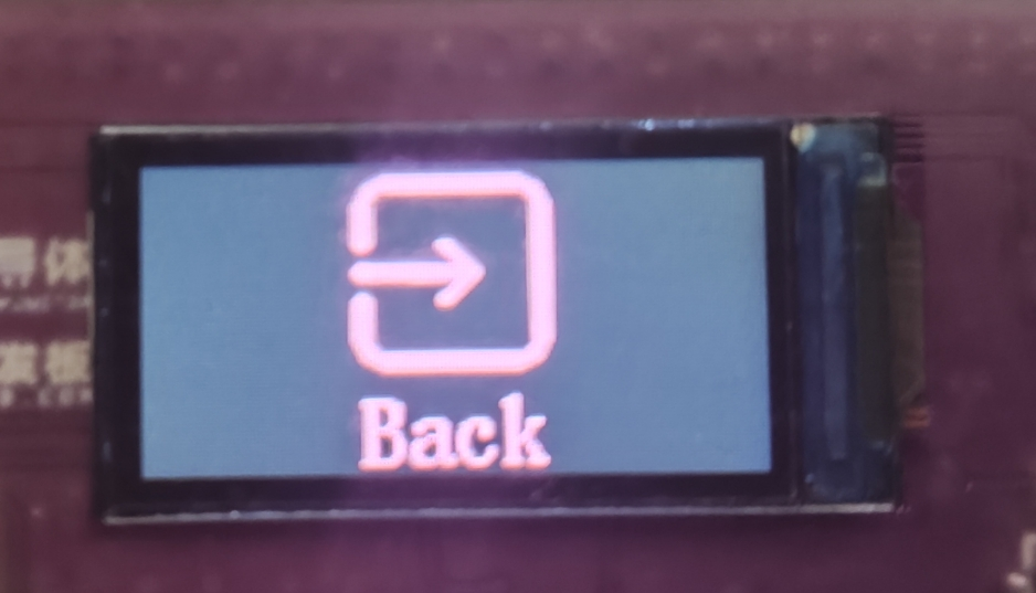
Press both buttons simultaneously to enter the function menu
; right-click to switch between coulomb meter interfaces
. In the coulomb meter interface, press the left button to clear the time and coulomb value
(pressing both buttons simultaneously will not trigger the left and right button functions).
UI Menu:
Left and right buttons switch menus;
pressing both buttons simultaneously confirms (back in the brightness adjustment interface).
When the screen flips, the buttons will flip accordingly,
returning to the main interface and saving the state to flash.
A flash equalization loss algorithm is used, theoretically with a lifespan of 1000 cycles, two bytes per cycle, and one sector (512 bytes) can save for 250,000 cycles.
Possible bug: One error may occur every 255 cycles (this bug is unverified and may not exist).
A key point about LCDConfig:
Due to differences in screen batches, some may have negative colors, while
others may have BGR. Use the "OK" button on this interface to switch until the screen icon colors are normal.
There are four configurations in total.
As for different XY offsets, this can only be resolved by modifying the program offset.
Function demonstration video: [Mini USB Voltage and Current Meter - Bilibili] https://b23.tv/0eSmw3u
Important Notes: When soldering headers
for 5A or higher interfaces
, ensure they are aligned correctly. Otherwise, they will not be level.
After soldering the headers, first test the functionality by attaching the development board to the headers, then solder them securely
. To ensure a smooth solder joint, see the image below. Solder two headers to empty I/O pins, using

screws and nuts as spacers. Buy the size shown below.

The printed panel is semi-transparent, and the text is very unclear. If you don't like it, adjust the transparency control layer yourself.
As for the 8A and 16A markings on the panel, just take it as a joke; those are the maximum register values.
16A requires replacing the sampling resistor, modifying the program, and also requires a 10A connector.
I. Design Background
An ADC (Analog-to-Digital Converter) is an indispensable key component in electronic systems. It converts continuous analog signals into digital signals, enabling digital processing and analysis. ADCs play a crucial role in signal conversion, measurement and data acquisition, control system input, and communication and signal processing. Their widespread application promotes the intelligent and precise control of electronic equipment across various industries, and is one of the key factors driving modern technological progress.
Digital voltmeters and ammeters combine ADC technology with circuit measurement principles, accurately converting analog voltage and current signals into digital displays for easy reading and analysis by electronic engineers. This device not only improves the accuracy and efficiency of circuit measurements but also helps engineers better understand circuit behavior, making it a powerful tool for electronic design and troubleshooting, and playing a vital supporting role in the work of electronic engineers. In product applications, digital voltmeters ensure the accuracy and safety of circuit design, while also providing strong support for product quality control and subsequent maintenance. Learning to design and build a digital voltmeter and ammeter
using a benchtop digital multimeter (Agilent 34401A)
is highly beneficial for improving one's professional skills. This digital voltmeter and ammeter project covers multiple aspects, including microcontroller circuit design and implementation, signal acquisition and processing circuit design, user interface development and optimization, and product appearance design. It integrates knowledge from multiple fields such as electronics, microcontroller programming, circuit design, and industrial design. Considering the learning pace and knowledge absorption capacity of beginners, we have specially launched this introductory-level digital voltmeter and ammeter project, which is very suitable for beginners in electronics and those who want to learn more about microcontroller applications. This project has the following highlights:
it adopts a core board plus expansion board design concept and uses plug-in components, making learning simpler and exploration more in-depth;
the core board uses the domestic Wuhan Xinyuan Semiconductor CW32 as the main controller, while also being compatible with other similar development boards; however, the CW32 has advantages.
The project is highly comprehensive and practical, and after completion, it can be used as a desktop instrument;
the project has abundant learning materials, including circuit design tutorials, PCB design, code programming learning, and training for engineers' debugging skills.
II. Hardware Design
1. Power Supply Circuit

LDO (Low Dropout Linear Regulator) Selection This project uses an LDO as the power supply. Considering that most voltmeter products are used in industrial scenarios with 24V or 36V power supplies, the SE8550K2 with a maximum input voltage of up to 40V was selected as the power supply. The main reason for not using a DC-DC step-down circuit to handle the large voltage drop is to avoid introducing DC-DC ripple interference during the design process, and the secondary reason is to reduce project costs.
2. MCU Selection Analysis
To reduce the learning cost for everyone, this project uses the LCSC CW32F030C8Tx development board (core board) as the main controller, but this does not mean that we will talk less about this section. From the perspective of training engineers, the correct selection of the main controller is very important, as it relates to the overall advantage of the project. Regarding the voltmeter and current meter, the author used STM32/CW32 and some other 32-bit microcontrollers for some debugging and testing. This comparison is only with the STM32F103C8T6 as a reference for device selection, primarily aimed at providing ideas and improving understanding.
Avoid blind selection. When selecting an MCU (Microcontroller Unit) for this project, multiple aspects need to be considered to ensure the chosen MCU meets project requirements.
Clearly define your project needs: Understand the required computing power, including clock speed, processor core type, and whether a floating-point unit is needed.
Identify the required I/O ports and important peripherals, such as ADC peripherals. Since this is a development board project, primarily for debugging and learning, there are no strict limitations on the number of I/O ports: i.e., the associated costs are not considered.
Key advantages of the CW32 in this project
: Wide operating temperature range: -40~105℃;
Wide operating voltage range: 1.65V~5.5V (STM32 only supports 3.3V systems)
; Superior interference immunity: HBM ESD 8KV; All ESD reliability meets the highest international standard (STM32 ESD 2KV)
; Project focus - Better ADC: 12-bit high-speed ADC, achieving ±1.0LSB INL 11.3ENOB; Multiple Vref reference voltages... (STM32 only supports VDD=Vref);
Stable and reliable eFLASH technology.
A detailed explanation of these advantages will be provided in the chapters on ADC sampling and related extensions.
The main characteristics of the CW32 ADC: This project requires a focus on the 4 reference voltage sources. (Content from the "CW32x030 User Manual")

3. Voltage Sampling Circuit:
The voltage divider resistors in this project are designed to be 220K+10K, therefore the voltage division ratio is 22:1 (ADC_IN11).
The voltage divider resistor selection
is designed to measure the maximum voltage. For safety reasons, this project uses 30V (the actual maximum display value can be 99.9V or 100V).
The ADC reference voltage is 1.5V in this project, and this reference voltage can be configured through the program.
To reduce the power consumption of the sampling circuit, the low-side resistor (R7) is usually chosen as 10K based on experience.
Then, the high-side resistance of the voltage divider resistor can be calculated using the above parameters.
The required voltage division ratio is calculated, i.e., the ADC reference voltage. The input voltage is designed; using known parameters, 1.5V/30V = 0.05 can be calculated.
The high-side resistance is calculated as the low-side resistance/voltage division ratio; using known parameters, 10K/0.05 = 200K can be calculated.
A standard resistor is selected: a resistor slightly higher than the calculated value of 200K is chosen. We usually choose E24 series resistors; therefore, in this project, 220K, which is greater than 200K and closest to the calculated value, is selected.
If, in actual use, the voltage to be measured is lower than 2/3 of the module's design voltage (66V), the voltage divider resistor can be replaced and the program modified to improve measurement accuracy. The following example illustrates this:
Assuming the measured voltage is no higher than 24V and other parameters remain unchanged,
calculations show 1.5V/24V = 0.0625, 10K/0.0625 = 160K. 160K is a standard E24 resistor and can be directly selected, or a higher value 180K can be chosen with some redundancy.
If, in actual use, the voltage to be measured is higher than the module's 99V design voltage, a different resistor can be selected. To expand the voltage measurement range, you can choose to replace the voltage divider resistor or modify the reference voltage. The following example illustrates this:
Assuming the measured voltage is 160V, we can choose to increase the voltage reference to expand the range.
Given that the voltage division ratio of the selected resistor is 0.0145, we can calculate 160V * 0.0145 = 2.32V using the formula. Therefore, we can choose a 2.5V voltage reference to expand the range (increasing the range will reduce accuracy).
Considering the potential fluctuations in the measured power supply, a 10nF filter capacitor is connected in parallel with the low-side voltage divider resistor in the circuit design to improve measurement stability.
(Range switching )
In this project, an additional voltage sampling circuit was added. Therefore, we can discuss the significance of range switching for improving measurement accuracy. Multimeters often have multiple range settings to achieve more accurate measurements. By adjusting different ranges, the optimal measurement accuracy of the measured point within the corresponding range can be obtained.
This project requires a combination of hardware and software to implement this function. When we first use the ADC_IN11 channel mentioned earlier to measure voltages below 30V, if the measured voltage is within 0~3V, then we use the ADC_IN9 channel for measurement. At this time, due to the reduced voltage division ratio, the measurement accuracy is greatly improved. There are many ways to implement range switching; the development board design provides more design possibilities.
4. Current Sampling Circuit
This project uses a low-side current sampling circuit for current detection. When learning the common ground between the low-side of the sampling circuit and the development board's meter interface, please do not solder R0!!!

The design analysis
for this project involves a sampling current of 3A, and the selected sampling resistor (R0) is 100mΩ. The selection of the sampling resistor mainly needs to consider the following aspects:
the maximum value of the pre-designed measurement current;
the voltage difference caused by the 3A current sensing resistor in this project; and
the power dissipation of the current sensing resistor, which should generally not exceed 0.5V. A suitable package should be selected based on this parameter. Considering the power dissipation (temperature) issue under high current, a 1W metal wire-wound resistor package was chosen
. The voltage amplification factor across the current sensing resistor is also important. Since no operational amplifier is used to build the amplification circuit in this project, the factor is 1.
The current sensing resistor value can then be calculated using the above parameters
. Since no amplifier circuit is used, a larger sampling resistor is needed to obtain a higher measured voltage for measurement.
Considering that a larger resistor would result in a larger voltage drop and higher power consumption, an unlimited selection of a larger resistor is not feasible.
This project uses a 1W package resistor, corresponding to a power consumption of 1W.
Based on the above data, a 100mΩ current sensing resistor was selected. According to the formula, 3A * 100mΩ = 300mV, 900mW can be calculated.
To cope with different operating environments, especially high-current scenarios, the R0 resistor can be replaced with constantan wire or a shunt. The replacement can be selected according to the actual application scenario. For safety and educational purposes, this project will not discuss measurements exceeding 3A in detail, but the principle is the same.
5. Digital Tube Display
This project uses a digital tube as the display unit.

This project uses two 0.28-inch three-digit common-cathode LED displays as the display device. Compared to a display screen, LED displays offer better visibility in complex environments. The brightness of the LED displays can be increased by using smaller current-limiting resistors, depending on the specific needs of the application environment. Furthermore, LED displays have better mechanical properties and are not as easily damaged by external forces as display screens. They are widely used in industrial applications where stability and reliability are crucial. From a development board learning perspective, this makes it easier to learn electronic measurement principles and related development in a targeted manner.
In this project, actual testing showed that the current-limiting resistors (R1~R6) for the LED displays were configured to 300Ω. The corresponding brightness for both red and blue LED displays was good and the brightness was soft and not glaring.
Strictly speaking, the current-limiting resistors should be added to the segments; adding them to the digits would affect the display effect. Our actual design places them in the digits to save a few resistors, but the impact on the display is not significant. Therefore, we add them to the digits for convenience.
The

driving principle of LED displays mainly involves controlling the switching state of each segment of the LED display to display numbers, letters, or symbols. The following is a detailed explanation of the driving principle:
Basic Structure of a Digital Tube:
A digital tube typically consists of seven or eight LED segments (eight segments in this project). Each segment represents a part of the digital tube and can display numbers 0-9, letters AF, etc.
Digital tubes come in two types: common cathode and common anode. The difference lies in whether the common terminal COM (the end connecting all LEDs) is connected to the negative or positive terminal of the power supply.
Driving Methods:
Segment Selection: The desired number or character is displayed by controlling the on/off state of each segment of the digital tube. Each segment corresponds to a control signal; when the control signal is on, the segment lights up, and vice versa. (a, b, c, d, e, f, g, dp)
Bit Selection: The digital tube to be displayed is selected by controlling the bit lines of the digital tube. Bit line control sets the bit line of the digital tube to be displayed to a high level, and the bit lines of other digital tubes to a low level. By continuously switching the state of the bit lines, the display switching between multiple digital tubes can be achieved.
Driving Circuit:
The driving circuit for a digital tube can be implemented using hardware circuits, such as integrated circuits like digital signal processors (DSPs), microcontrollers (MCUs), or shift registers, to generate control signals suitable for the LEDs.
These control signals can be in the form of pulse width modulation (PWM) signals, serial data signals, etc. By controlling the frequency, width, and amplitude of these signals, the brightness of the digital tube can be controlled, thereby displaying the desired numbers or letters.
Software Control:
In addition to hardware driving circuits, the driving of digital tubes can also be implemented through software control. By programming to generate control signals suitable for the digital tubes, more flexible and complex display effects can be achieved, such as scrolling or alternating display of numbers.
Driving Common Cathode and Common Anode Digital Tubes:
For common cathode digital tubes, the common cathode pin is connected to the negative terminal of the power supply, and the control pin is connected to the output pin of the control chip. When a certain number needs to be displayed, the control chip outputs the corresponding encoded signal to the control pin, causing the corresponding LED segment to light up.
For common anode digital tubes, the working principle is similar to that of common cathode digital tubes, except that the common anode pin is connected to the positive terminal of the power supply, and the control pin is connected to the output pin of the control chip.
Encoded Display:
In order for the digital tube to display the corresponding numbers or characters, the segment data port must output the corresponding character encoding. For example, to display the number "0", the character code for a common anode seven-segment display is 11000000B (i.e., C0H), while the character code for a common cathode seven-segment display is 00111111B (i.e., 3FH). The specific code depends on the actual seven-segment display.
Dynamic and Static Display:
Seven-segment displays can use either static or dynamic display methods. In static display, each of the eight segments of each seven-segment display is connected to an 8-bit I/O port address. As long as the I/O port outputs a segment code, the corresponding character is displayed and remains unchanged. Dynamic display, on the other hand, lights up each segment of the seven-segment display one by one, achieving simultaneous visual display through rapid switching.
In summary, the driving principle of seven-segment displays is to control the switching state of each segment of the seven-segment display to display numbers, letters, or symbols, and to achieve display switching between multiple seven-segment displays through segment selection and digit selection. Furthermore, the driving of seven-segment displays can be implemented through hardware circuits or software control, and common cathode or common anode seven-segment displays can be selected as needed.
This project actually uses dynamic scanning display to drive the seven-segment display.
To estimate the current required for the digital tube display,
this project actually uses dynamic scanning to drive the digital tubes. Therefore, at any given time, only a maximum of 8 segments of the digital tube (or LEDs) can be lit, or in other words, only one digit can be lit. According to the design, the required driving current is approximately 11mA, which is the high-level voltage of the I/O port: 3.3V ÷ 300Ω.
At this point, it is important to ensure that the selected MCU has sufficient current-source/current-sinking capability.


Analysis of the datasheet shows that the CW32 has no issues. (Some chips do not work.)
6. LED Indicators
This project additionally designed a power indicator and an I/O operation indicator.

LD_PWR is the power operation indicator

. Since the chip's I/O often has a greater current sinking capability than a current pulling capability, LED1 is designed to be active low (on).
To reduce the current consumption of the LED, some LED brightness is sacrificed, the number of component parameters is reduced, and the current-limiting resistor for the LED is selected as 10K.
7. Button Circuit Design

There are various design methods for the button control circuit. Thanks to the fact that the CW32's I/O port can be configured with pull-up and pull-down resistors internally, the button control circuit on the outside of the chip does not need to be configured. One end of the button is connected to the MCU's I/O, and the other end is grounded. When the button is pressed, the I/O is pulled low.
8. TL431 Circuit Design for Voltage Measurement and Calibration:
This project adds an extra TL431 circuit to provide a 2.5V reference voltage. This can be used to provide an external voltage reference for the chip to calibrate the AD converter. From a product design perspective, due to the inherent ADC performance advantages of the CW32, this circuit is not necessary. This circuit is designed on the development board to learn the relevant application principles.

The TL431 is a relatively "old" device, a classic, and widely used one, still found in many electronic products.
Many beginners may be encountering this device for the first time, so we will briefly explain its principles to help everyone better apply the TL431.
TI defines it as a "Precision Programmable Reference." On the first page of the references, we can focus on several key characteristics.
Precision: Precision indicates that its output voltage is very accurate. I used a ±0.5% accuracy TL431, which measured 2.495V on the board at room temperature. Compared to common Zener diodes, the accuracy is vastly different. In the application circuit diagram, the TL431 is represented by a Zener diode symbol.
Adjustable Output Voltage: The adjustable output voltage is between Vref and 36V. In our project, we use the output Vref voltage, which is approximately 2.5V. Therefore, we use 2.5V in the description, which is approximately equal to Vref.
Sinking Current Capability: This refers to how much current the output voltage pin can provide. This is greatly influenced by the resistance value (R13) in the application circuit. It should not be less than 1mA. If there is no need for sinking current, do not design the current to be too high, as this will cause unnecessary power consumption.
This project developed a voltmeter and ammeter capable of detecting voltages from 0-30V and currents from 0-3A, based on a CW32 microcontroller. The core function of the system is to acquire voltage and current signals via an ADC (Analog-to-Digital Converter) and then accurately process and display these signals. To improve measurement accuracy, the project employed a calibration data method to calibrate and process the acquired raw data, thereby reducing errors and improving the accuracy of the measurement results.
In terms of hardware, the voltage and current detection ranges are 0-30V and 0-3A, respectively, covering the needs of most everyday applications. The system utilizes a high-precision ADC module to convert analog signals into digital signals for subsequent software processing. The software relies on the powerful processing capabilities of the CW32 microcontroller, combined with calibration data, to correct the acquired digital signals, ensuring the accuracy and reliability of the final displayed voltage and current values.
The calibration process involves acquiring multiple known voltage and current values, recording the corresponding ADC values, and generating a calibration curve or lookup table. During actual measurement, the system interpolates or corrects the raw data based on the values acquired by the ADC, referencing the calibration data, thereby outputting accurate measurement results. The entire process ensures that the system maintains high-precision measurement performance under various environments and conditions.
Furthermore, the system features an intuitive user interface that displays voltage and current values in real time and provides basic alarm and protection functions, guaranteeing both safety and ease of use.
In summary, this voltmeter and ammeter project fully considers measurement accuracy, system stability, and user experience in its design, making it suitable for voltage and current monitoring needs in a variety of applications.
#LCSC Training Camp# A voltage and current meter designed based on the CW32F030C8T6 development board, making full use of available components and changing the through-hole component to a surface-mount component.
PDF_#LCSC Training Camp# Voltage and Current Meter Designed Based on CW32F030C8T6.zip
Altium_#LCSC Training Camp# Voltage and Current Meter Designed Based on CW32F030C8T6.zip
PADS_#LCSC Training Camp# Voltage and Current Meter Designed Based on CW32F030C8T6.zip
BOM_#LCSC Training Camp# Voltage and Current Meter Designed Based on CW32F030C8T6.xlsx
 Background: When debugging serial communication in a project, serial communication tools are needed, sometimes TTL, sometimes RS232, and sometimes RS485. Using separate communication tools inevitably involves plugging and unplugging devices, which is cumbersome.


 An AP63203 DC-DC converter is used, with a fixed 3.3V output. However, this power supply design had a slight mishap. The AP63203 DC-DC datasheet states a 3.3V output, but the actual output is about 0.1-0.3V higher, causing the ST7735 screen to display incorrectly when the input voltage is high. Fortunately, the solution is simple: short-circuit the 3.3V and 5V on the development board. Testing showed that after short-circuiting, the output was 3.4V with a 20V input, but this did not affect operation.
  main control MCU
  See source code: https://gitee.com/xmqor/cw32f030-mini-usb-voltage-ammeter
  Coulomb meter: The coulomb meter samples power 100 times per second via a timer and calculates the integral.
  UI menu:
 UI operation instructions:
 2. Power supply.
  components include: 3. Voltage sampling circuit;
  4. Current sampling circuit and current measurement port
  ; 5. Voltage calibration;
  6. Current calibration; 7.
  Digital tube display;
  8. Buttons and indicator lights ;
  9. Drawing the PCB and placing the training camp logo and Chip Source logo;
  10. Designing the casing;
  11. Designing the faceplate; 12. PCB fabrication
  and soldering;
  13. Assembling the casing
  . The faceplate design was finished, but I forgot to place the order. Just make do with it. There's still a lot of room for improvement.


 京公网安备 11010802033920号

 MI-Q2Y-IVY


