1. Name of the contestant: Fan Ang
2. Name of the company or school: Siemens
3. Current position or title: Supervisor
4. Name of the entry: Portable CNC power supply for debugging
5. Briefly state your idea and work (required):
Working range: Input AC220V +-10%, output 0...30V adjustable, current 0...0.8A adjustable
Adopts isolated flyback switching power supply structure, high efficiency, primary and secondary isolation
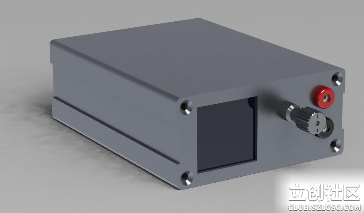
Small size, roughly equivalent to a mobile hard disk, easy to carry
Built-in user-friendly HMI, LCD display, encoder adjustment
With additional and secondary development functions, such as battery charging, VI adjustable curve output, 4..20mA current source, industrial field signal source, etc.
6. Materials sold in LiChuang Mall to be used (required):
STM32F051C8
PC817C
Rotary encoding switch EVE-VCGJL016B
KF5N60F
7. Materials not sold in LiChuang Mall to be used or other supplements:
1.8-inch LCD module
EFD25 transformer
8. EDA tool software name to be used: LCEDA
9. Original link: http://club.szlcsc.com/article/details_16056_1.html
10. Original project link: https://oshwhub.com/arokh/dcp3001
I. Introduction to the work
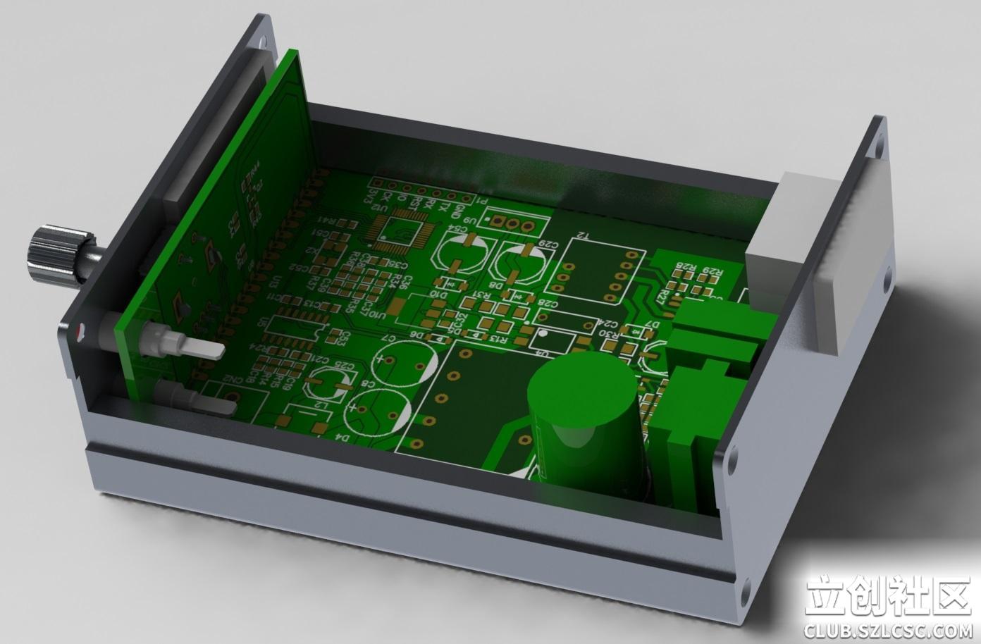
1. Design concept diagram

2. Actual picture
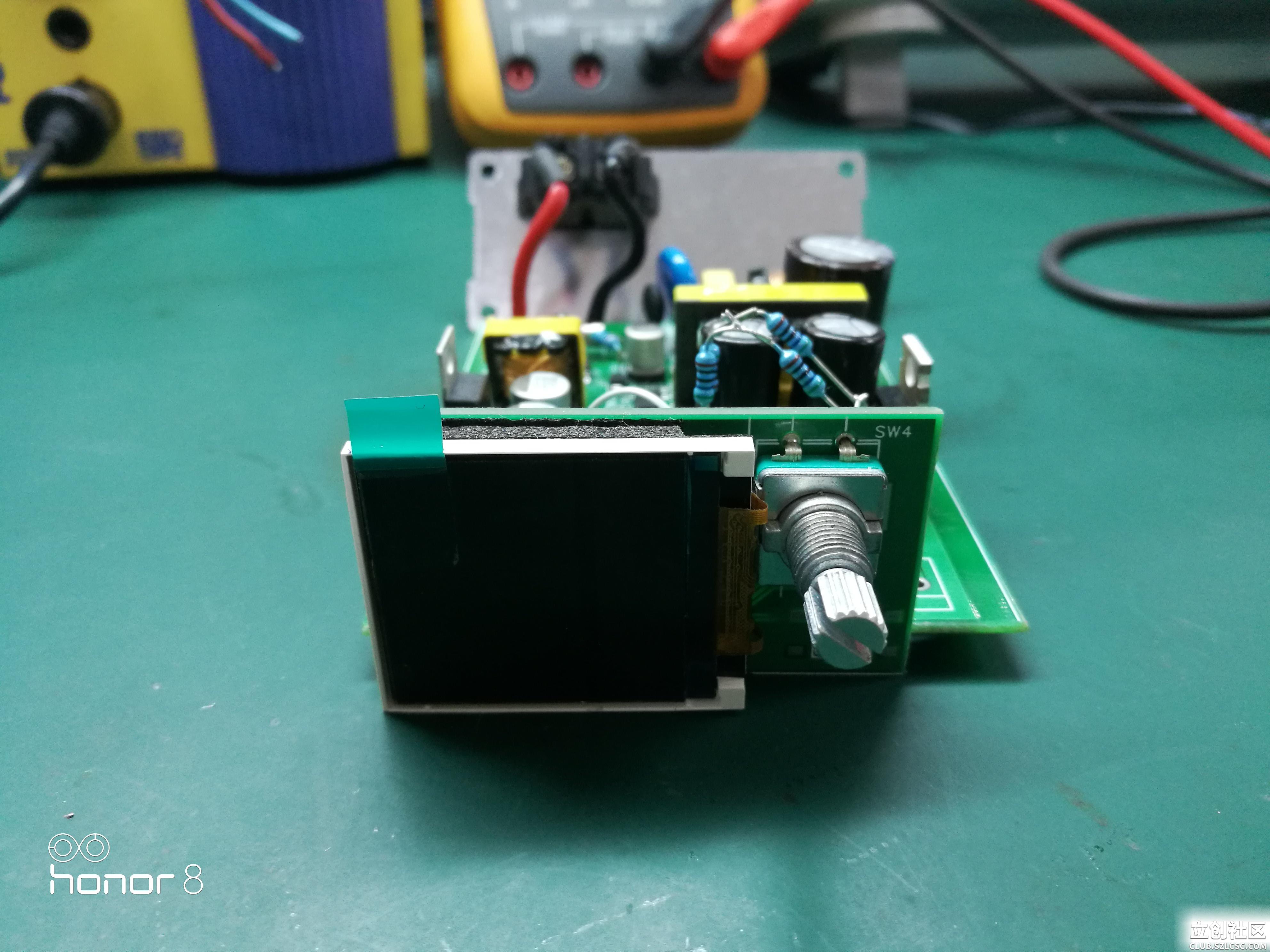
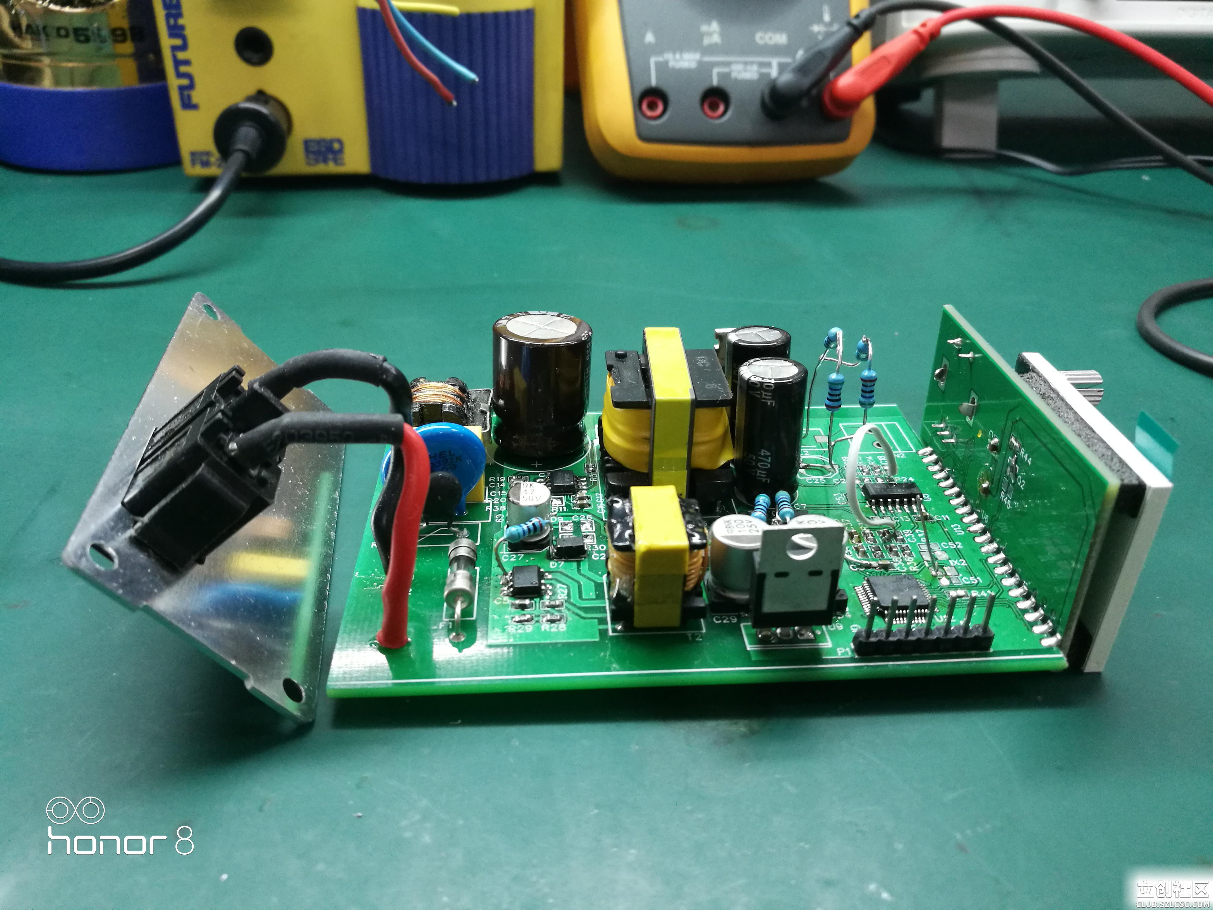

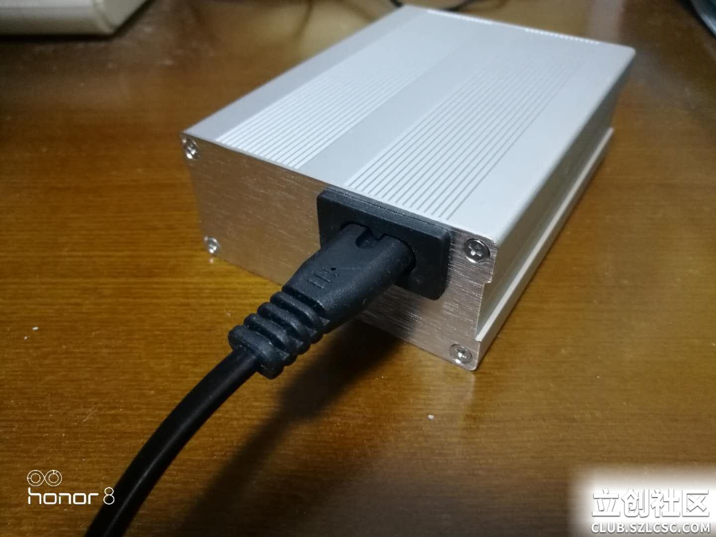
Special reminder here: The safety distance between the primary and secondary sides is not enough in the current state! Do not imitate!
3. Research background, purpose and function of the work, and market application prospects:
At present, the debugging power supply on the market mostly adopts the structure of power frequency transformer plus power tube linear price reduction, with a power output range of 0~30V3~5A, and focuses on accuracy; but the disadvantage is that it is large in size and heavy in weight and inconvenient to carry. I need a small power of 0~30V1A, not particularly high in accuracy, and portable power supply for on-site debugging. Similar products on the market have large power and single function.
Therefore, the key features of this entry are set as "multi-function", "portable" and "switch type". The market prospects are mainly for engineers with needs like mine.
4. What are the highlights of the work in terms of innovation, fun, practicality and even public welfare?
The human-machine interface uses TFT LCD instead of the traditional seven-segment digital tube, which can provide more information (such as curve display). After opening all information, it has stronger secondary development potential. The operation uses a rotary encoder, which is convenient and fast. The parameter adjustment is proportional to the rotation speed (the faster you turn it, the faster the parameter changes, showing an exponential curve), and the user experience is better.
The shell is made of aluminum alloy profiles, and the LCD screen is also a standard size, which is convenient for procurement. It is very convenient for everyone to DIY or imitate in the future.
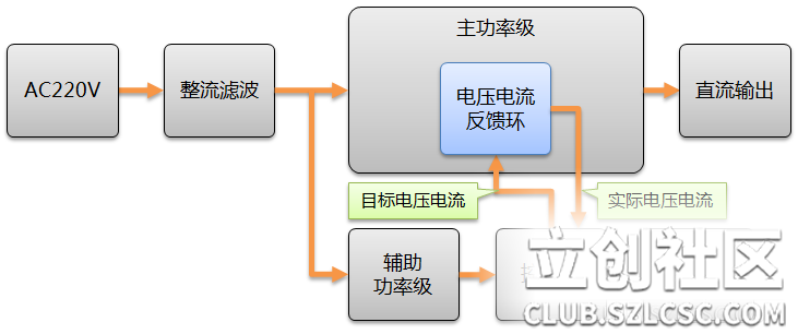
2. System architecture diagram
Principle structure block diagram:
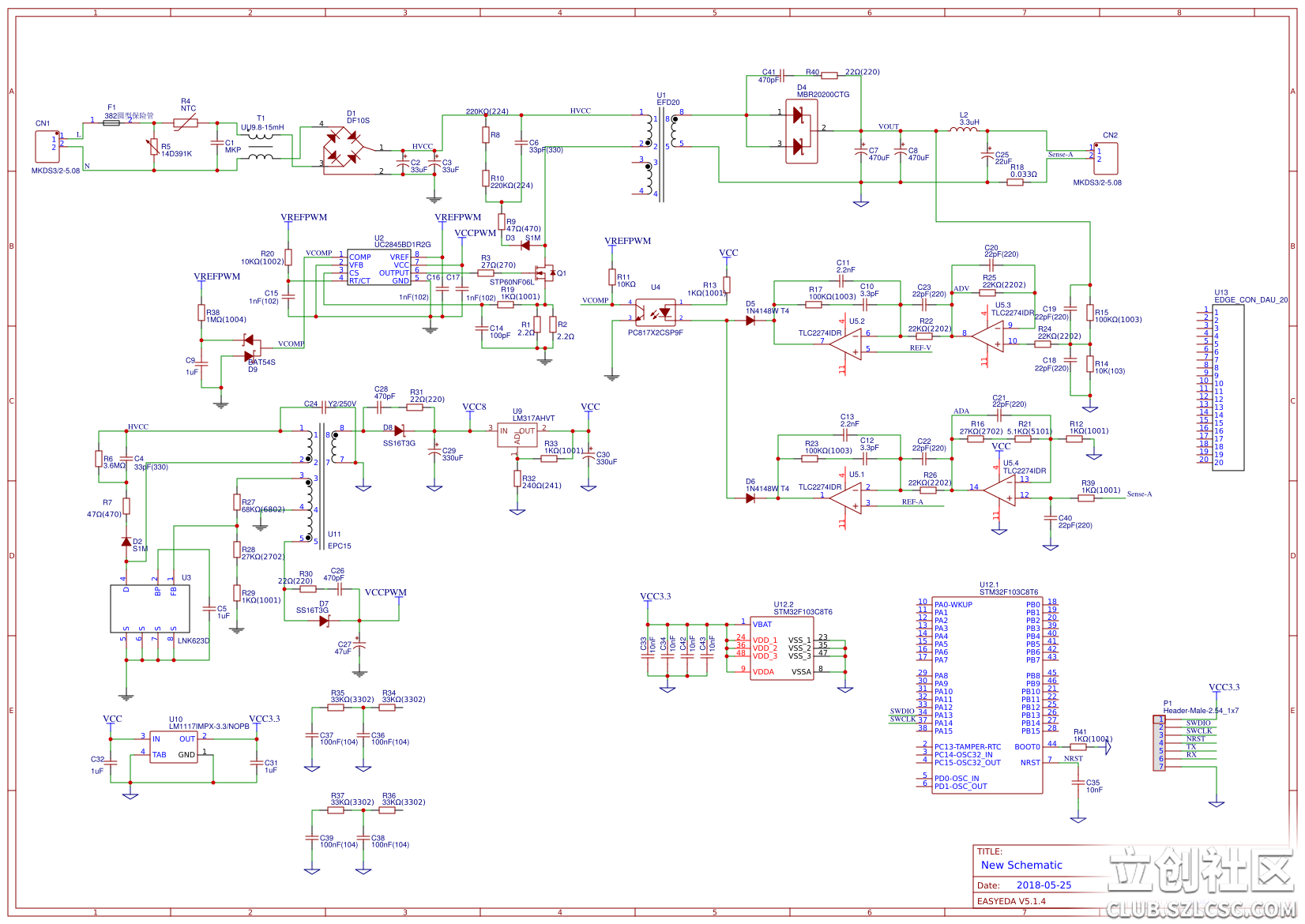
3. Description of the hardware part
This design uses LCEDA, which is very fast to get started and is extremely suitable for the design and implementation of this work.
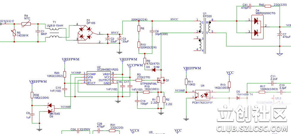
Schematic diagram:

PCB:
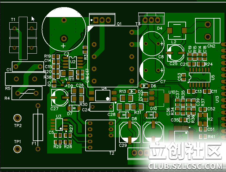
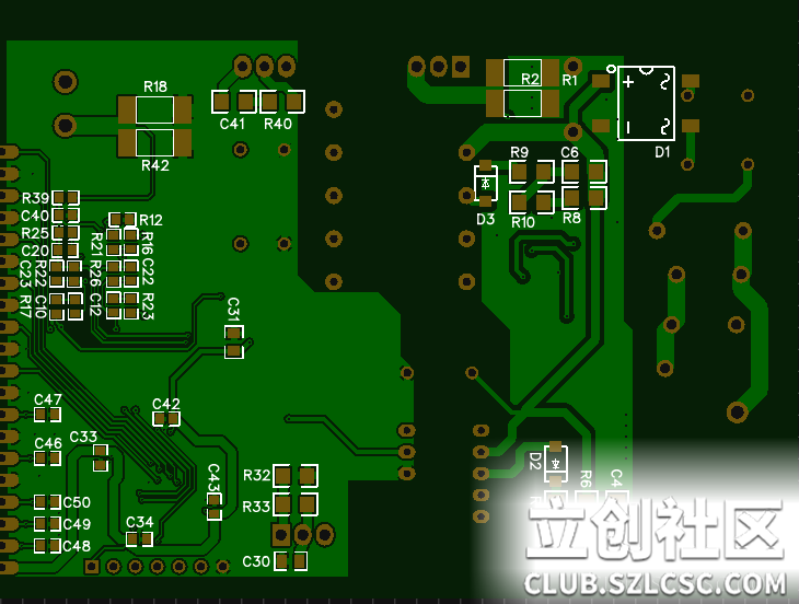


http://club.szlcsc.com/article/downFile_C05AA4E03ACF07C3.html
A few considerations:
1. This power supply is only a CNC power supply rather than a digital power supply, so the feedback loop is still in analog form. The CNC part completes the voltage and current setting and calibration.
2. Safety, I was entangled in the grounding problem. Considering the heat dissipation, I want to use an aluminum alloy shell. If the power socket is grounded, it will be very large. For the time being, consider internal double insulation first, and then talk about it if it doesn't work.
Block description:
1. Auxiliary power supply part:
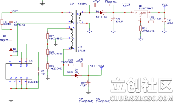
Considering that the characteristics of the auxiliary power supply are low power, multiple outputs, and isolation, the flyback topology is specially selected.
The solution uses PowerInt's LNK62x, which has a simple structure and low cost. The solution is mature and is widely used in home appliances.
In addition, the supplier of this solution provides a complete automated design tool PIExpert, which is very convenient for design optimization.
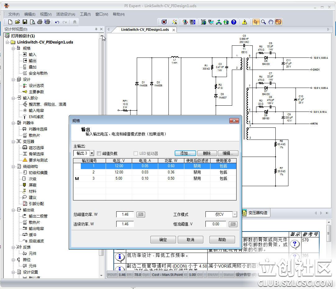
The transformer uses EE13 core and 5+5 skeleton according to the structural limitations and the number of output channels. The transformer design output by the software is for reference only. On this basis, I have further optimized the primary and secondary side creepage distance and pin allocation. See the schematic diagram for detailed allocation.
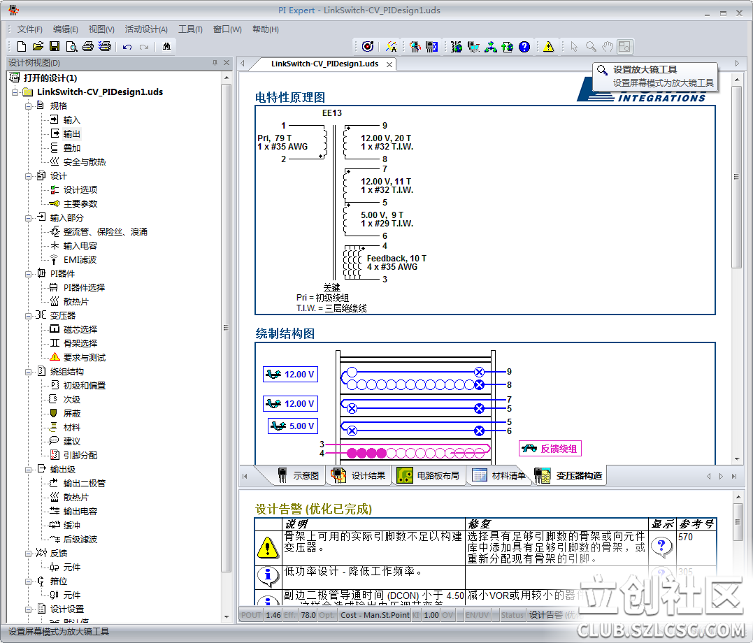
Attached design engineering file: LinkSwitch-CV_PIDesign1.rar (Downloads: 497)
2. Main power stage:
This part still uses the classic flyback structure. The main controller is also the classic UCx845. I believe that friends who are familiar with power supplies are already familiar with the IC x845, so I will not go into detail about the design.
The following is a screenshot of my homemade flyback design gadget (due to various reasons and copyright reference issues, it is inconvenient to share the source file, please forgive me).
If you need to use the UCx845 automatic design tool, I recommend TI's Webench, which is also very convenient!
Input and output parameter settings:


transformer parameters (except for the incorrect air gap, other parameters are almost the same). There are actually some problems with the RC absorption circuit, which need to be corrected:
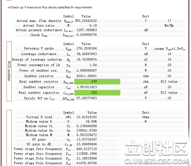
Use EXCEL to draw the power level Bode diagram
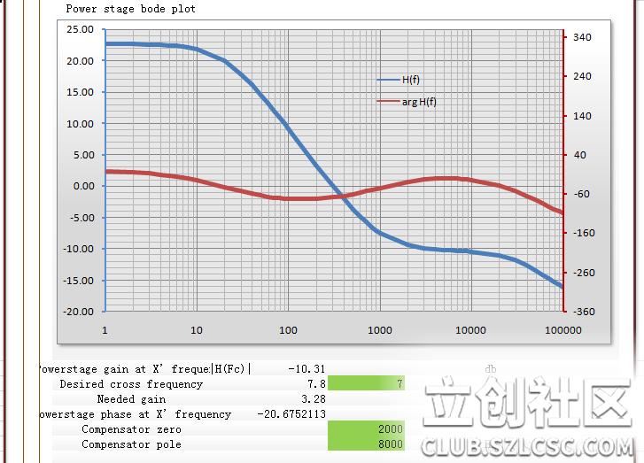
to adjust the compensator, and the compensated Bode diagram (not yet fine-tuned):
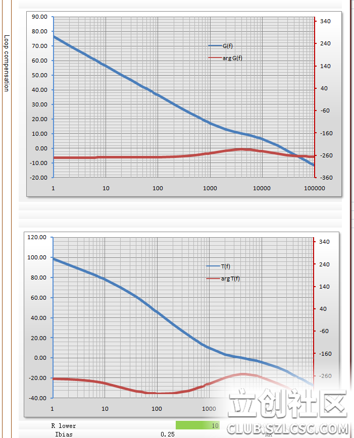
I personally think that the switching power supply is three-point design and seven-point debugging. Although the work in the design stage must be done, there are actually quite a lot of variables, and more effort is needed for later debugging.
3. Voltage and current feedback loop:
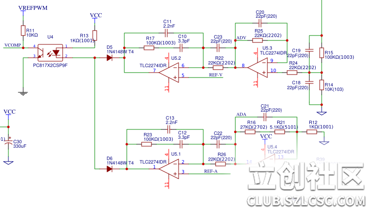
This part of the circuit is my "Spring Breeze Power Supply" (I bow to my predecessor here!), and I have made some changes based on my understanding.
The upper part is the voltage loop, and the lower part is the current loop. The two parts drive the optocoupler after being "wired-OR" through the diode.
The structures of the two parts are actually the same. After the voltage and current are sampled, they first pass through the first-stage 0dB drive, and then output to the second-stage TYPEII compensator for compensation and optocoupler drive.
Not all capacitors in the figure are required, and the parameter values are still to be refined and adjusted.
It is particularly important to note that the first-stage TYPE I capacitor and the subsequent TYPE II compensation should not exist at the same time. Otherwise, multiple poles will be superimposed (>-40dB attenuation)
4. Bill of Materials (BOM List)

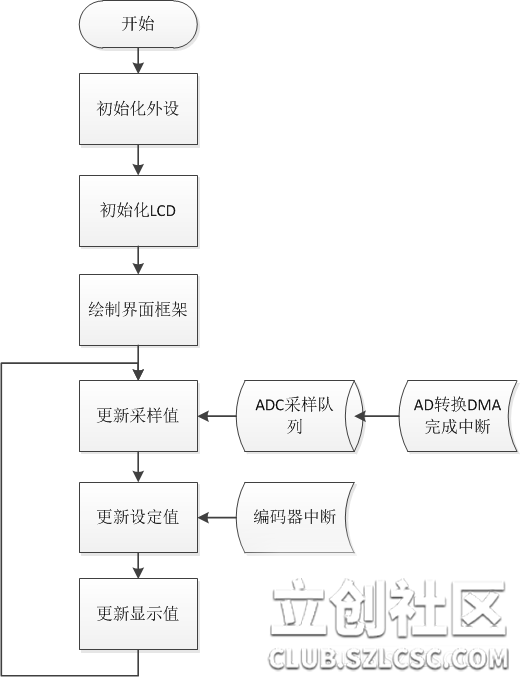
5. Description of the software part (optional)

DCP3001_V01.rar (Downloads: 809)
6. Work Demonstration
Video Link: http://v.qq.com/x/page/j0757r8o0ep.html
7. Summary
When using PIExpert to design a transformer, the parameters were changed but not re-optimized, resulting in incorrect transformation ratio, high reflected voltage, and stuck for two days;
ADC sampling seemed to encounter aliasing problems, and low voltage could not be measured. Time is too tight this time, so let's do the function first. If we improve it later, we will add a low-pass filter to filter out the switching frequency;
the feedback loop will not oscillate with the value calculated for the first time. In order to verify it, the compensator was removed, and the Vds waveform shook decisively. I will go online and adjust it carefully when I have time. The purpose of building a loop experimental platform this time has been achieved; the
schematic diagram will be updated later, and the time node cannot be given at present;
as a middle-aged greasy uncle, there are too many trivial matters, and it is difficult to calm down and do some hobbies. I don’t know if I can participate next time. Anyway, I have tried my best this time; for
more project details, please see the link: http://club.szlcsc.com/article/details_16056_1.html
This project belongs to the LiChuang community "arokh"


 京公网安备 11010802033920号

 PNM2512E20R3DST5


