Open the official website of Tuya Smart, register a developer account, and click Create Product: 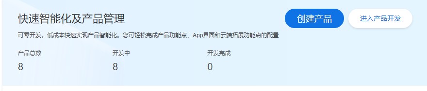 Then you can see a lot of options. Because we chose the free development plan this time, we need to find the free development plan of the air-conditioning companion among the various options. Development options. As shown in the figure:
 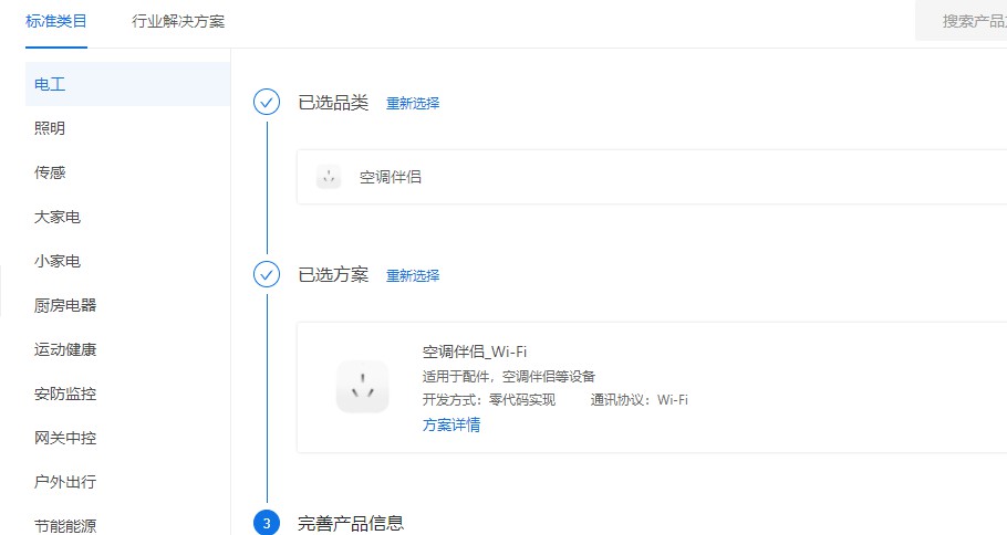 confirm the project name and desired communication method. The next step is to select the required functions, because what we are making is an air conditioner infrared remote control plus night light, you can select it as needed. The next step is to choose the APP control interface. Tuya provides us with many optional interfaces, so we don’t need to write the APP ourselves, which is very convenient and fast. As shown in the picture:
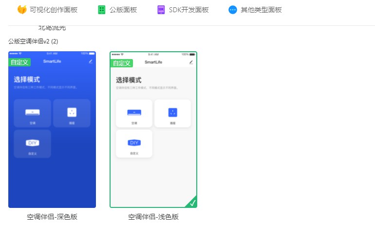
After it is determined, it is the hardware debugging part. Here we need to adjust each GPIO interface according to the required functions. Because we have chosen a development-free solution, we do not need to write the code ourselves. Everything can be done by the Tuya platform. We only need to simply Just select the pin you want to control. It should be noted here that two functions cannot be assigned to the same pin port. As shown in the picture, I just use the default one: 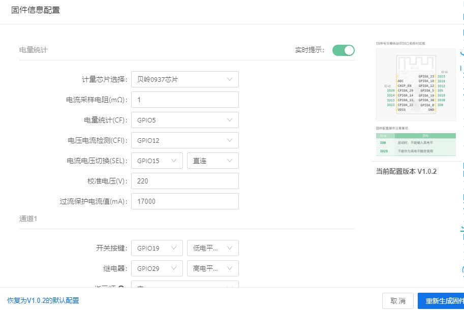 After completing this step, you can place an order to purchase the module. Tuya Platform 18 also comes with free shipping, which is very cost-effective.
After the module arrives, we can start to complete the drawing of the PCB. It is also very easy because we have already selected the function of each pin above. Here we only need to connect the corresponding pins to the actuator. , such as: the infrared pin is connected to the control part of the IR LED, the network indicator light is connected to the LED, etc. This is my schematic diagram, which implements infrared sending, infrared learning, night light control and other functions: 
It can be seen that it is very simple. This schematic diagram was drawn using Lichuang EDA and with the help of a rich component library, it was completed very quickly. The next step is to convert the schematic diagram to PCB. There is not much to say about this. They are all low-speed and low-voltage lines. Basically, as long as the connection is OK, it can work normally. This is my PCB picture. What needs to be paid attention to here is the wifi communication. Try not to route wires and attach copper under the module, as this will affect the communication distance. This is my PCB picture: 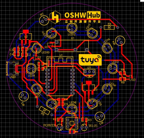 after checking it, it can be sent to the PCB factory for production, and the soldering can be completed after receiving the board. Before turning on the power, check whether the power supply voltage meets the requirements and whether there is any tin connection during welding.

All reference designs on this site are sourced from major semiconductor manufacturers or collected online for learning and research. The copyright belongs to the semiconductor manufacturer or the original author. If you believe that the reference design of this site infringes upon your relevant rights and interests, please send us a rights notice. As a neutral platform service provider, we will take measures to delete the relevant content in accordance with relevant laws after receiving the relevant notice from the rights holder. Please send relevant notifications to email: bbs_service@eeworld.com.cn.
It is your responsibility to test the circuit yourself and determine its suitability for you. EEWorld will not be liable for direct, indirect, special, incidental, consequential or punitive damages arising from any cause or anything connected to any reference design used.
Supported by EEWorld Datasheet
EEWorld
subscription
account

EEWorld
service
account

Automotive
development
community

Robot
development
community

About Us Customer Service Contact Information Datasheet Sitemap LatestNews


Room 1530, 15th Floor, Building B,
No.18 Zhongguancun Street,
Haidian District,
Beijing, Postal Code: 100190
China
Telephone: 008610 8235 0740
 京公网安备 11010802033920号

 2SC184