First of all, I would like to apologize to the friends who made the last version of the board, because when I made this soldering iron, I just wanted to use the screen of Tun, and I did not expect to open source it, nor did I expect that after the open source mini heating table, my friends would become more Pay attention to my soldering pen, so I made a version with a 0.5-inch screen that is available on the market, so that interested friends can make their own soldering iron. Secondly, let’s talk about the original intention of making this electric soldering iron. I still remember that the first electric soldering iron I owned more than ten years ago was an external heating type that cost more than ten dollars. Later, I used an internal heating type. After using it for a long time, it became dull. When dipping tin, a handy tool is very important. I wonder how old it is. How come the electric soldering iron still looks like an electric soldering iron? Can't it be as portable as a pen? It happens to come into contact with the T12 soldering iron tip and the small-sized and high-power nitrogen soldering iron. For a gallium charger, if it has a hard core, it must be given a transparent casing so that each component can be clearly seen. This must be the favorite of every science and engineering man, and I am even more looking forward to the large-scale application of transparent PCBs. one day.
Let’s look at some model pictures next.
Finally, I highly recommend friends who like it to make one themselves. The cost will not exceed a hundred, and it is also commemorative. What you buy is a commodity after all. I am also very grateful to Jialichuang for the service support provided, from PCB design to From prototyping, component procurement, and 3D printing, I can achieve creative freedom in front of the computer.
In view of the pitfalls that I have encountered during the production process and the problems that my friends may encounter, I have sorted them out. There may be some that I have not considered. Friends can write them in the comment area and we will promptly update them after seeing them. Reply, I don’t plan to set up an exchange group at the moment, because I still have school work, and I don’t have the energy to do this for the time being, so I will write it in as much detail as possible so that novices can follow the tutorial. Attached is the link to the previous version of the tutorial video https ://www.bilibili.com/video/BV1Wq4y1Y7PS?share_source=copy_web
| Component name | Precautions |
| shrapnel | The raw material is the pole piece of the CR1220 battery holder. You need to use scissors and pliers to modify the shape. |
| 0402 SMD 4.7uf capacitor | Be sure to choose one with a voltage resistance of 25V |
| buzzer | SMD 5020 Passive SMD Buzzer |
| 26M crystal oscillator | SMD3225-4P, pay attention to the direction when welding, there is a triangular notch on pin 1 |
| Four indicator lights in series with resistors | Currently it is 470Ω. You can also change it to other suitable resistance values, but the brightness will be different. |
| 4.7uH power inductor | The model is SWPA252012S4R7MT. You can choose Lichuang Mall C87640 or Taobao. |
| 0.5 inch OLED | You can find it on Lichuang Mall and Taobao, 88*48 CH1115 driver IIC |
| Master chip | When choosing esp8266, you need to solder W25Q32. When choosing esp8285, you don’t need to solder. It is recommended to use 8285 to save money. |
| touch chip | Compatible with TTP223 and PT2042AT6 |
| Precision operational amplifier | Compatible with GS8551 and SGM8551XN5G/TR in SOT-23-5 package |
You can solder the whole board first and then separate the board with a hook knife, but be careful not to cut the circuit. You can also separate the board first and then solder it individually. This method is recommended for novices . Weld the components of the front patch first, then weld the buzzer and female base on the back, then weld the spring piece, and finally weld the screen. When welding the screen, the FPC solder joints should be small.
After each board is powered on and tested correctly, perform three-dimensional welding of the triangular prism. First, insert the three boards into the auxiliary positioning block for positioning. Adjust the position. Weld the half hole at the tail first. It is best not to weld it firmly at once, leaving some The room for adjustment is like tightening multiple screws. Don't tighten one at a time. Apply a little tin first, and then add more tin to solder it firmly after the triangular prism structure is determined.
Use Arduino to burn the program. Before that, you need to compile it and add library files, otherwise there will be a compilation error. First install the ESP8266 development board library. I uploaded the offline installation package (8266_package_2.7.4.exe) in the attachment. Just double-click to run it. After installation, restart Arduino and select the development board, as shown in the figure below. If you are using 8285, select For 8285, use 8266 for 8266. There is a difference between the two when burning.
Install the library file, as shown in the figure below. Add the .ZIP library in the attachment. You can also click Manage Library and search for online installation.
After the compilation is successful, burn it. Use a TTL downloader to connect to the onboard TX, RX, 3V3, and GND. I used a homemade ESP8266 downloader. I aimed it at the four solder points and pressed and held to burn. Anyway, I only used it once. OTA will be used for subsequent burning. Before burning, enter the download mode. Use tweezers to short-circuit the two solder joints of IO0 and hold them. At the same time, use another tweezers to short-circuit the two solder joints of RST and then disconnect them. Then disconnect the short-circuit of IO0. Then the burning begins.
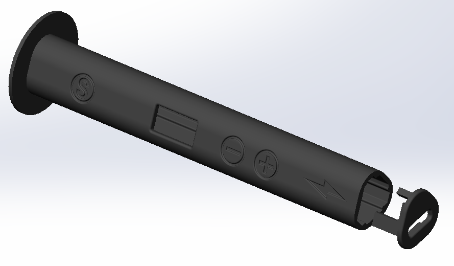
The original design was to use a disposable glue package as the shell. The biggest advantage of this is that it is small in size and hard-core cool. However, it is troublesome to make. It requires a silicone mold and sealing. It takes several days to solidify and the success rate is also very low. Later, It also needs to be polished, and the touch buttons should be used under sealed conditions (this is also a pit). So I took a step back and tried to 3D print a detachable shell if it was not transparent. Although there are also transparent materials, I don’t recommend it for those who don’t have a printer (I asked one shop and it cost 100+). I first made a sample, made of white photosensitive resin, mainly to test whether the size would fit, as shown in the picture below.
Sure enough, the inner cavity is a bit big, but this is not a problem. Just make some modifications. Now that our school is closed, we don’t have a printer and the express delivery is super slow, so there is no opportunity for iterative modifications. I hope that friends with stereolithography printers around me can help. I verified it (see the attachment for the STL file). It is not recommended to use an FDM printer because it has a thin wall and a slender shaft structure. The hot bed attached to the bottom is not strong and the surface accuracy is not high, even though I increased the bottom attachment area. The shell printing model is shown in the picture below. It contains two parts, the shell and the shell cover. In order to increase the attachment area during printing, an auxiliary round plate is added to the shell. Just cut it off after printing is completed.
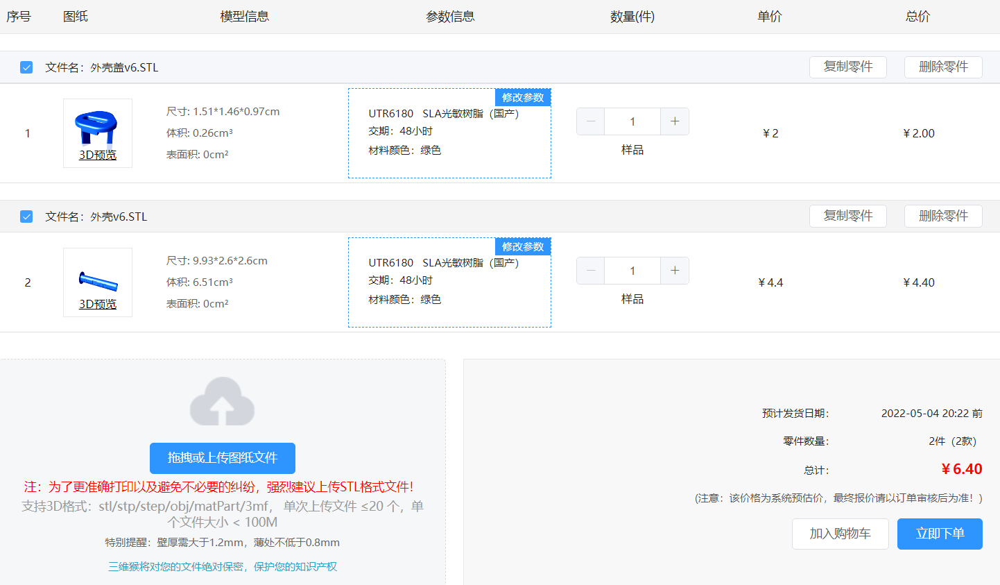
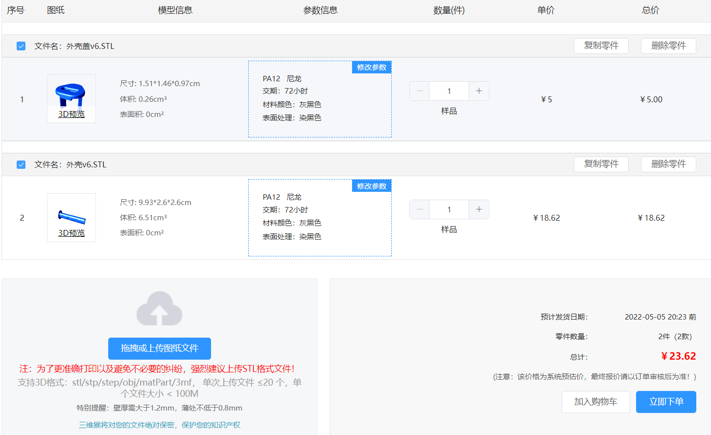
I also tried to place an order on 3D Monkey and chose URT6180 photosensitive resin and PA12 nylon as shown in the picture. I did not choose white because it was too ordinary.
In the past, the shell sealed with glue was in direct contact with the touch pad, so as long as a capacitor with a suitable capacitance value was used, a suitable touch sensitivity could be achieved. However, there is an air medium between the detached shell and the touch pad, so the capacitor is Adjusting the capacitance value to the minimum and the highest sensitivity is far from enough. This will result in the touch pad inside being unable to be touched through a layer of shell (it’s over, that’s not useless). Fortunately, a medium was finally found - nanometer Traceless glue (single-sided), cut a piece of suitable size and stick it on the touch pad to reduce the gap between it and the shell, which perfectly solves the problem of touch capacitance.

All reference designs on this site are sourced from major semiconductor manufacturers or collected online for learning and research. The copyright belongs to the semiconductor manufacturer or the original author. If you believe that the reference design of this site infringes upon your relevant rights and interests, please send us a rights notice. As a neutral platform service provider, we will take measures to delete the relevant content in accordance with relevant laws after receiving the relevant notice from the rights holder. Please send relevant notifications to email: bbs_service@eeworld.com.cn.
It is your responsibility to test the circuit yourself and determine its suitability for you. EEWorld will not be liable for direct, indirect, special, incidental, consequential or punitive damages arising from any cause or anything connected to any reference design used.
Supported by EEWorld Datasheet
EEWorld
subscription
account

EEWorld
service
account

Automotive
development
community

Robot
development
community

About Us Customer Service Contact Information Datasheet Sitemap LatestNews


Room 1530, 15th Floor, Building B,
No.18 Zhongguancun Street,
Haidian District,
Beijing, Postal Code: 100190
China
Telephone: 008610 8235 0740
 京公网安备 11010802033920号


 1825400-3


