The USB ammeter made based on N32G430C8L7+INA199 has an accuracy of 1%. You can check the current when USB is working. The project is divided into two versions, one is an ammeter that supports fast charging, and the other is a 5V meter that does not support fast charging display.
This project is used for training camp case teaching projects. It does not support fast charging and can only measure a maximum voltage of 6V. If you need to support fast charging, please modify it yourself!
The N32G430C8L7 microcontroller product uses a high-performance 32-bit ARM Cortex™-M4F core, integrates a floating-point unit (FPU) and digital signal processing (DSP), and supports parallel computing instructions. The maximum operating frequency is 128MHz, it integrates up to 64KB of on-chip encrypted storage Flash, supports multi-user partition permission management, and supports 16KB of embedded SRAM. Built-in an internal high-speed AHB bus, two low-speed peripheral clock buses APB and bus matrix, supports 40 reusable I/Os, provides rich high-performance analog interfaces, including a 12-bit 4.7Msps ADC, supports 16 external Input channels and 3 internal channels also provide a variety of digital communication interfaces, including 4 U(S)ART, 2 I2C, 2 SPI/I2S, and 1 CAN 2.0B communication interface. The N32G430C8L7 microcontroller product can stably operate in the temperature range of -40°C to +105°C, with a power supply voltage of 2.4V to 3.6V, and provides a variety of power consumption modes.
This case does not use many resources. The internal clock has been open sourced to meet the design requirements, so there is no need for an external clock circuit. It should be noted that each power supply pin of the chip needs to be connected to an additional 100nF external filter capacitor , and pin 1 of the chip needs to be connected to an additional 4.7uf filter capacitor .
Since this design is designed to fit the public version of the casing, the reset circuit and BOOT circuit are not designed with buttons, and two solder joints are used as short circuits.
The chip supports a variety of burning methods, such as ST-Link, USB-TTL, Jlink and other common burners on the market. In the case, the corresponding interface uses a 2.54 pitch pin header for programming.
Although the MCU used in this case supports a maximum voltage of 5V, considering that the USB voltage or other voltages may have unstable voltage factors, a 6V to 3.3V LDO is used to power the chip. Even if the power supply is not available, Under stable conditions, the MCU can also work normally. It should be noted that the LDO input and output must be connected to 22uF and 100nF capacitors.
The USB input terminal uses a Type-A male connector, and the input voltage is 5V. This interface supports a maximum output of 3A. If it is larger, it will be a bit hot. It is recommended not to exceed the current of 3A. If you need to use a larger current, please replace the Type-A male connector.
The USB output terminal uses a 4P sinking plate female socket. In order to adapt to the public version of the housing, the maximum rated current of this female socket is 1.5A. The actual measured current is 2.5A, but it is not suitable for long-term operation at this current. If necessary If you use a larger current, please replace it yourself.
The current sampling part is the INA199B1DCKR current sense amplifier, (also called a current sense amplifier) which is often used for overcurrent protection, precision current measurement for system optimization, or closed-loop feedback circuits. This family of devices senses the voltage drop across a shunt resistor at a common-mode voltage of –0.3V to 26V, independent of the supply voltage. There are three fixed gains to choose from: 50V/V, 100V/V and 200V/V. This family of devices uses a zero-drift architecture with low offset to maintain the maximum voltage drop across the shunt resistor to a minimum of 10mV full-scale when sensing current. The parameters are as follows:
Inserting a low-value sense resistor in series with the current path creates a small voltage drop that is amplified and treated as a signal proportional to the current. However, this technique will pose different challenges to the sense amplifier depending on the application environment and the location of the sense resistor. Generally, the resistance value of the sampling resistor is below 1 ohm, which is a milliohm-level non-inductive resistor. However, some resistors have sampling voltage and other requirements, so a resistor with a large resistance value must be selected, but the resistance base is large and the error is large. In this case, it is necessary to choose a high-precision non-inductive resistor (which can reach 0.01% accuracy, that is, one ten thousandth of an accuracy) to make the sampling data very reliable. SMD ultra-low resistance value resistors (0.0005 ohms, 2 milliohms, 3 milliohms, 10 milliohms, etc.), chip alloy resistors, high-power resistors (20W, 30W, 35W, 50W, 100W) and other products, temperature coefficient It is plus or minus 5PPM.
Note: If the stock of INA199B1DCKR is insufficient, you can replace the INA199A3DCKT chip. It should be noted that the magnification of INA199B1DCKR is 50. If you use other magnifications, you need to re-modify the program calibration.
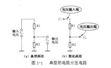
The voltage sampling part consists of a voltage dividing circuit composed of two resistors. The principle is based on the knowledge of voltage dividing by resistors in series. The typical circuit is as follows:
The display part uses a 0.91-inch 4P white OELD screen module, using IIC communication, and the display effect is clear.
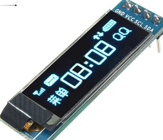
Design display effect
If the sampled voltage or current is inaccurate, you can modify the sum value main.cin the file based on the actual value . The specific calculation formula is:VOLTAGE_FACTORCURRENT_FACTOR
VOLTAGE_FACTOR = 实际电压 / 显示电压
CURRENT_FACTOR = 实际电流 / 显示电流
Finally, we would like to thank our open source enthusiasts micespring for their software support.
Source project reference: https://oshwhub.com/micespring/USBmeter
# Update log - August 23, 2022 A new program has been uploaded to fix the overlapping of characters when the display digits exceed 3 digits. ![image.png]

All reference designs on this site are sourced from major semiconductor manufacturers or collected online for learning and research. The copyright belongs to the semiconductor manufacturer or the original author. If you believe that the reference design of this site infringes upon your relevant rights and interests, please send us a rights notice. As a neutral platform service provider, we will take measures to delete the relevant content in accordance with relevant laws after receiving the relevant notice from the rights holder. Please send relevant notifications to email: bbs_service@eeworld.com.cn.
It is your responsibility to test the circuit yourself and determine its suitability for you. EEWorld will not be liable for direct, indirect, special, incidental, consequential or punitive damages arising from any cause or anything connected to any reference design used.
Supported by EEWorld Datasheet
EEWorld
subscription
account

EEWorld
service
account

Automotive
development
community

Robot
development
community

About Us Customer Service Contact Information Datasheet Sitemap LatestNews


Room 1530, 15th Floor, Building B,
No.18 Zhongguancun Street,
Haidian District,
Beijing, Postal Code: 100190
China
Telephone: 008610 8235 0740
 京公网安备 11010802033920号


 1-147741-7


