## Table of Contents **1. Preface** **2. Team Introduction** **3. Question Requirements** **4. Question Analysis** **5. Schematic Design Instructions** **6. PCB Design Description** **7. Software description** **8. Physical display description** **9. Notes** **10. Test results** ## 1. Preface This work is the 2021 National Electronic Design Competition The entry for Question A was well completed and finally won the first prize in the Shaanxi Provincial Competition Area and the second prize in the country. ## 2. Team introduction This team is composed of three students from the School of Electrical Engineering of Xi'an Jiaotong University. The author himself is responsible for the design and production of analog circuits, and classmate Zhou Wei in the team is responsible for writing digital programs. Android APP is written using the App inventor platform. ## 3. The question requires the design and production of a signal distortion measurement device to collect and analyze the periodic signal (hereinafter referred to as the input signal) from the function/arbitrary waveform generator, and measure the total harmonic distortion THD (hereinafter referred to as the input signal) of the input signal. distortion), and can display measurement information on the mobile phone. **1.Basic requirements:** (1) Peak-to-peak voltage range of input signal: 300mV~600mV; (2) Fundamental frequency of input signal: 1kHz; (3) Input signal distortion range: 5% ~ 50%; ( 4) The absolute value of the input signal distortion measurement error is required to be less than 5%; (5) The distortion measurement value THD is displayed; (6) The distortion measurement and display time does not exceed 10 seconds. **2. Play part:** (1) Peak-to-peak voltage range of the input signal: 30mV ~ 600mV; (2) Fundamental frequency range of the input signal: 1kHz ~100kHz; (3) Measure and display the input signal distortion THD value, The required error is ≤3%; (4) Measure and display a periodic waveform of the input signal; (5) Display the normalized amplitude of the fundamental wave and harmonics of the input signal, and only display the 5th harmonic; (6) On the mobile phone It displays the THD value of the input signal measured and displayed by the measuring device, a periodic waveform, the normalized amplitude of the fundamental wave and harmonics. ## 4. Question analysis According to the question, the design should follow the process from signal collection to digital processing, and finally display the results. **So the design should contain three parts:** (1) Signal conditioning and other necessary analog circuits; (2) Digital control scheme of the controller; (3) Bluetooth and Bluetooth app. **Analysis of analog circuit design:** Signal distortion calculation requires two types of data: waveform and signal frequency. Therefore, the analog circuit should include two parts: signal conditioning circuit and shaping circuit. The function of the signal conditioning circuit is to convert the 30-600mV bipolar signal required by the question into a voltage signal (0-3.3V) that the on-chip ADC can accept. The solution of fixed gain amplifier + DC bias can be used, which is simple in structure and does not consume time. However, the disadvantage is that the ADC sampling error is large when small signals are input, the measurement accuracy is limited, and the measurement amplitude range is difficult to increase. Therefore, we adopted the AGC (automatic gain control amplifier) + DC bias solution, which can output the input signal with a constant amplitude and greatly increase the measurement signal amplitude range. However, the disadvantage is that the production is time-consuming and debugging is complicated. The function of the shaping circuit is to obtain a square wave with the same frequency as the fundamental wave of the input signal. **Analysis of the digital processing solution:** The front-end analog circuit provides a square wave with the same frequency as the fundamental wave, and the microcontroller can use the input capture of the timer to measure its input fundamental wave frequency. Then the sampling rate is determined based on the fundamental frequency, and the on-chip ADC is used to sample the waveform signal. Finally, after obtaining the periodic voltage data, FFT is used to calculate the harmonic components and THD. One thing worth noting is that due to the limitation of the on-chip ADC sampling rate (most of TI's processors are around 1M), there is a large gap between the 100KHz waveform signal obtained by direct sampling and the actual waveform, so the direct sampling solution is not advisable. Therefore, our group’s plan is to use undersampling, that is, to collect data for one period in multiple periods. For example, 1024 points need to be collected in one period. The first point is sampled in the first period, and the second point is sampled in the second period. A point... **Analysis of the Bluetooth display solution:** The question does not have high requirements for this part. It is enough to be able to use Bluetooth to send data to the mobile phone and display it. Therefore, it is best to use a more mature Bluetooth module (such as HC05), and the APP design is also simple. It is recommended to use app inventor (visual module programming). ##
Tips: Overall design block diagram
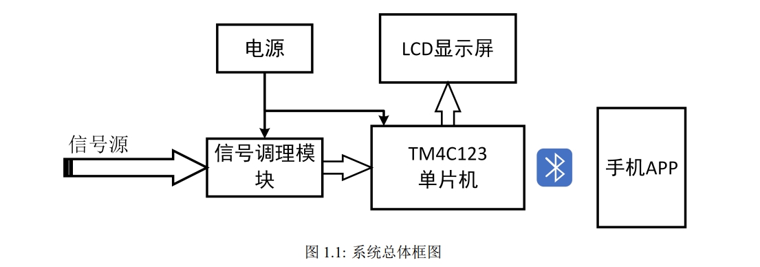
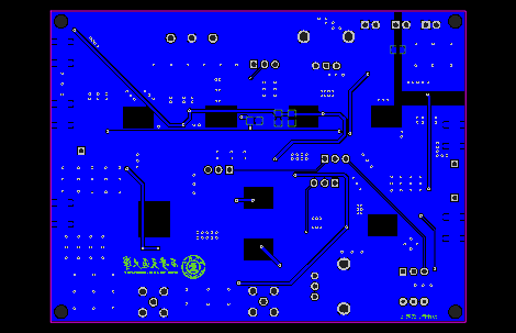
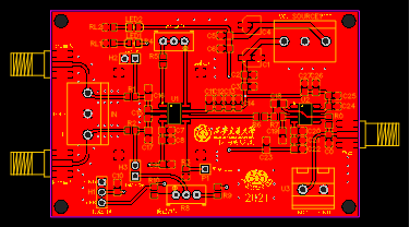
## 5. Schematic design description **The work has five parts in total:** (1) Power bus (in the middle of the physical picture): A multi-terminal interface containing positive and negative power lines and ground wires is welded using a universal board, so that It makes the power supply of the system more convenient and troubleshooting power supply faults faster; (2) Fundamental wave shaping circuit (upper left corner of the actual picture): including the preamplification filter module (blue) and the post-stage shaping circuit (red), The signal is received from AGC, fixed gain, filtered and then shaped into a square wave with the same fundamental frequency; (3) Signal conditioning circuit-AGC (upper right corner of the actual picture): There is an automatic gain control circuit based on VCA821 in the blue PCB, and it is equipped with There is a DC bias circuit that can provide a constant waveform signal for the 0-3.3V on-chip ADC; (4) TI microprocessor and supporting display (lower right corner of the actual picture): Tiva C series TM4C123 and 2.2-inch LCD screen; (5) Bluetooth module (right side of the actual picture): HC05 module. **1. Analog circuit design:**
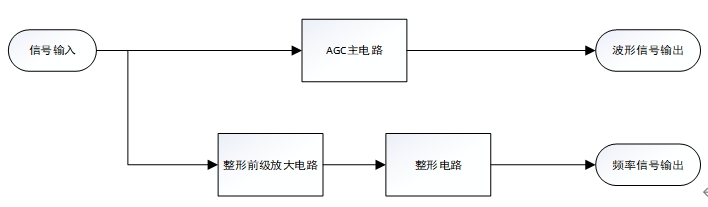
**The structure is divided into two channels:** The first channel: AGC + DC bias, output waveform signal; The second channel: shaping pre-stage (amplification and filtering) + square wave shaping, output frequency signal; **Performance introduction:** 1 .Amplitude range: input 5mVpp-4Vpp signal wave, constant output 3Vpp same waveform signal and same frequency square wave, matching the input range of the microcontroller ADC. However, when the amplitude is too low, the output amplitude will also decrease because the gain has a limit; 2. Frequency range: 1KHz-100KHz (the upper limit is limited by the AD620 in the shaping pre-stage circuit and the filtering link in the circuit, and the lower limit is limited by the AGC feedback branch Integration time of the integrator); **(1) Signal conditioning circuit design:**
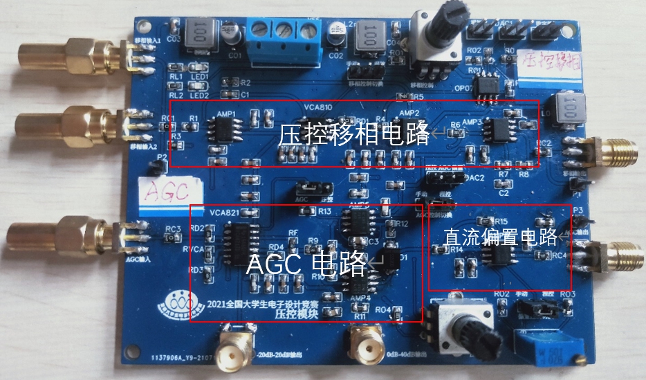
The module was made during my pre-competition training, so the PCB has an unused voltage-controlled phase shift circuit. This question only uses the AGC and signal bias circuit.
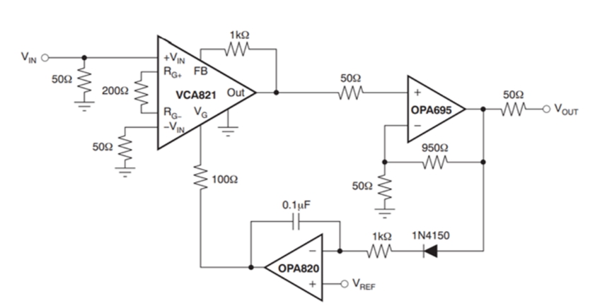
The picture above shows the closed-loop gain control circuit given in the VCA821 (voltage controlled amplifier chip) reference manual. The AGC main circuit structure used in this competition is the same as above. The difference is that the selection of op amps is not exactly the same as the above picture. In the above picture, opa695 is replaced by opa843, and opa820 is replaced by opa842. The use of opa695 (current mode operational amplifier) will cause self-excitation and various noise problems. This has been verified during the debugging process and is relatively difficult to use. Finally, the capacitor of the integrator must be connected in parallel with a 1M ohm resistor to prevent the zero drift of the amplifier from causing abnormal output. The selection of the integrator time constant depends on the actual situation. The smaller the time constant, the higher the lower frequency limit of the AGC. The integral constants on the PCB in the competition can only meet the control of signals above 800Hz. VCA821 has very advanced performance and a high frequency upper limit, so signals up to 10MHz can be processed. The DC bias circuit uses a subtractor to invert the input signal and input the DC signal in non-phase, so note: **The final waveform signal and the input signal are inverted! ** **(2) Shaping circuit design: ** In order to achieve the stability of small-amplitude signal frequency measurement square wave, the signal needs to be amplified and filtered in advance before shaping.
The amplifier circuit adopts the typical circuit of AD620, and the gain can be adjusted through the potentiometer above the area. The advantage of choosing AD620 is its high common mode rejection ratio. And the input resistance of the instrumentation amplifier is extremely high, which has little impact on AGC. But the disadvantage is that the frequency range is not high, and the higher the gain, the smaller the frequency range. This is one of the reasons why our group was unable to expand the frequency range later on. The filter circuit is designed as a second-order active filter with a cutoff frequency of 100KHz, which can be changed by replacing the resistor and capacitor.
It is also because the module is prepared during training, so it is not just the TLV3501 shaping circuit. The entire module has four parts, all of which are used for detection. The input has an opa843 as a buffer stage and a diode as input limiting, so the possibility of damage to the subsequent stage is less. **Includes:** (1) LM339 low-frequency shaping circuit; (2) TLV3501 high-frequency shaping circuit; (3) Peak detection circuit with TLV3501 and three-level operational amplifier as the core, the upper limit of the measurement frequency can reach tens of MHz, But the lower limit is also limited by the integral constant of the integrator; (4) The effective value detection circuit based on AD637 can control whether it works or not, and the upper limit frequency is 8MHz. This competition uses the TLV3501 high-frequency shaping circuit. **Hysteresis comparison circuit composed of TLV3501:**
**2. Digital circuit design:** The Tiva C development board is used and the SPI interface is used to connect the 2.2-inch LCD screen for display. The processor resources utilized are: 1. A timer input capture port (PB6) for frequency measurement; 2. An ADC sampling port for collecting waveform signals; 3. An SPI interface for connecting to the display; 4 .A serial port for connecting Bluetooth HC05. ## 6. PCB design instructions **AGC: **
**Shaping front-stage circuit:**
**TLV3501 shaping circuit:**
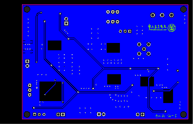
**Design points:** (1) Power line setting: The thickness meets the current demand, and the flow first passes through the filter capacitor and then to the device, etc.; (2) Power supply filter capacitor placement: Generally, one large and one small are placed on the power end of the device. , please refer to the layout of the relevant device manual; (3) Signal line layout: use arc corners and no sharp angles, the line width should be appropriately larger, reject parallel wiring, use as few through holes as possible, etc.; (4) Device placement: try to Make the devices evenly dispersed and the input pins of the main chip should be close to the input sma to avoid introducing additional interference; (5) Copper laying: The bottom PCB under the chip should be hollowed out to prevent stray capacitance from affecting the operation of high-frequency chips. ## 7.Software description
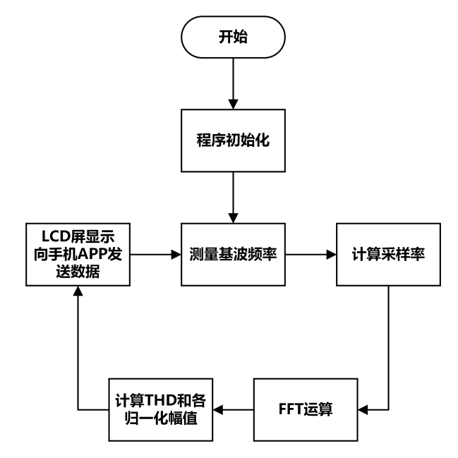
**The key is undersampling and FFT calculation, the specific content is as follows:** 1. **Frequency measurement**: Configure Timer1 for 1s and Timer0 for input capture mode, calculate the number of rising edges within 1s, and derive Input signal frequency; 2. **ADC sampling**: Determine the sampling rate according to different input signal fundamental frequencies, and the timer triggers ADC sampling; 3. **Total harmonic distortion (THD) and fundamental and harmonic normalization Measurement of harmonic amplitude**: Call the FFT function of the DSP library, perform a 1024-point FFT operation on the data collected by the ADC, and calculate the THD and normalized amplitude of each harmonic. **Code block:** ``` #define FFT_LENGTH 1024 //FFT points//uint32_t FFT_LENGTH = 1024; extern _lcd_dev lcddev; extern uint16_t pointcolor; extern uint16_t backcolor; extern uint8_t pressedKey; uint8_t key; uint16_t y_z[FFT_LENGTH]; uint8_t pui8ControlTable[1024]; arm_cfft_radix4_instance_f32 cfft; float input[FFT_LENGTH*2]; float output[FFT_LENGTH]; uint8_t timeout; uint32_t Data[FFT_LENGTH]; com=1 ; float freq_fund; //Fundamental frequency uint16_t freq_seq[5]; //Five frequency component index float32_t Uo[5]; //Five frequency component amplitude float THD; float norm_am[4]; uint16_t x_start; double freq = 0; uint32_t count=0, mycount=0; uint32_t Rate = 64000; void ADC0Sequence3Handler() { uint32_t ui32Mode; uint16_t i = 0; flag=0; for(i=0;iAIN11 ADCSequenceConfigure(ADC0_BASE,3,ADC_TRIGGER_TIMER,0 ; TIMER0_BASE,TIMER_CFG_PERIODIC); TimerLoadSet (TIMER0_BASE,TIMER_A,SysCtlClockGet()/Samp_rate-1); TimerADCEventSet(TIMER0_BASE,TIMER_ADC_TIMEOUT_A); TimerEnable(TIMER0_BASE,TIMER_A); ADCSequenceEnable(ADC0_BASE,3); ADCIntClear(ADC0_BASE, 3); } void InituDMA(void) { sCtlPeripheralClockGating (true); SysCtlPeripheralEnable(SYSCTL_PERIPH_UDMA); SysCtlPeripheralSleepEnable(SYSCTL_PERIPH_UDMA); IntEnable(INT_UDMAERR); uDMAEnable(); uDMAControlBaseSet(pui8ControlTable); uDMAChannelAssign(UDMA_CH17_ADC0_3); uDMAChannelAttributeDisable( UDMA_CHANNEL_ADC3,UDMA_ATTR_ALL); uDMAChannelControlSet(UDMA_CHANNEL_ADC3 | UDMA_PRI_SELECT,UDMA_SIZE_32 | UDMA_SRC_INC_NONE | UDMA_DST_INC_32 |UDMA_ARB_1); uDMAChannelTransferSet(UDMA_CHANNEL_ADC3 | UDMA_PRI_SELECT,UDMA_MODE_BASIC , (void *)(ADC0_BASE+ADC_O_SSFIFO3),Data,FFT_LENGTH); uDMAChannelAttributeEnable(UDMA_CHANNEL_ADC3,UDMA_ATTR_USEBUR ST); uDMAChannelEnable(UDMA_CHANNEL_ADC3); } void freq_measure() { uint16_t i, flag_1 = 1; float max = output[1]; for(i=1; i max) { max = output[i]; flag_1 = i; } } freq_fund = flag_1*((float)Rate/FFT_LENGTH); } float32_t THD_COMP () { uint8_t i = 0; float32_t sum = 0; float32_t Uo[4]; for(i=0;i<4;i++) { Uo[i] = output[4*i+8]/output[4] ; sum += Uo[i]*Uo[i]; } return 100.0*sqrt(sum); } float32_t my_THD_COMP() { uint16_t i, j, flag_1 = 1;; float max = output[1]; float max2, max3, max4,max5; for(i=1; i max) { max = output[i]; freq_seq[0] = i; } } Uo[0] = output[freq_seq[0]]; for(i=1;i<5 ;i++) { uint16_t hh; Uo[i] = output[freq_seq[0]*(i+1)]; hh = freq_seq[0]*(i+1); freq_seq[i] = freq_seq[0]*( i+1); for(j=1;j<8;j++) { if(output[hh-4+j]>Uo[i]) { Uo[i] = output[hh-4+j]; freq_seq [i] = hh-4+j; } } } for(i=0;i<5;i++) { UARTprintf("index = %d, U = %dn",freq_seq[i],(int)(Uo [i])); UARTprintf("index = %d, U = %dn",freq_seq[i]-1,(int)(output[freq_seq[i]-1])); UARTprintf("index = %d , U = %dn",freq_seq[i]+1,(int)(output[freq_seq[i]+1])); } for(i=0;i<5;i++) { if(Uo[i] /Uo[0] > 0.05f) { Uo[i] = sqrt(output[freq_seq[i]-1]*output[freq_seq[i]-1] + output[freq_seq[i]+1]*output[freq_seq [i]+1] + output[freq_seq[i]]*output[freq_seq[i]]); } } for(i=0;i<4;i++) { norm_am[i] = Uo[i+1] /Uo[0]; } float32_t sum=0.0f,thd1; for(i=0;i<4;i++) { sum+=Uo[i+1]*Uo[i+1]; } thd1 = sqrt(sum )/Uo[0]*100; return thd1; } ```
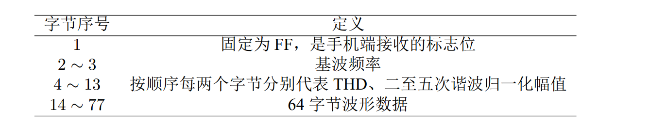
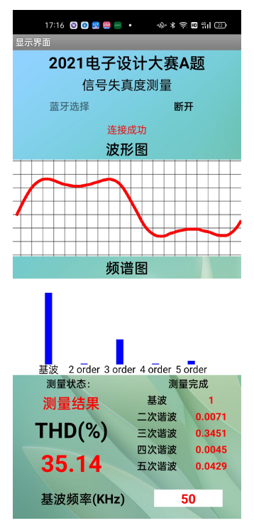
**Communication regulations between Bluetooth and mobile phones:** In terms of communication protocol, after each measurement, the MCU uses the serial port to cycle 5 times to send a 75-byte string to Bluetooth (directly using the corresponding characters of the ASCII code).
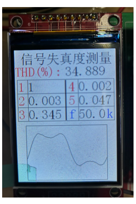
## 8. Physical display instructions
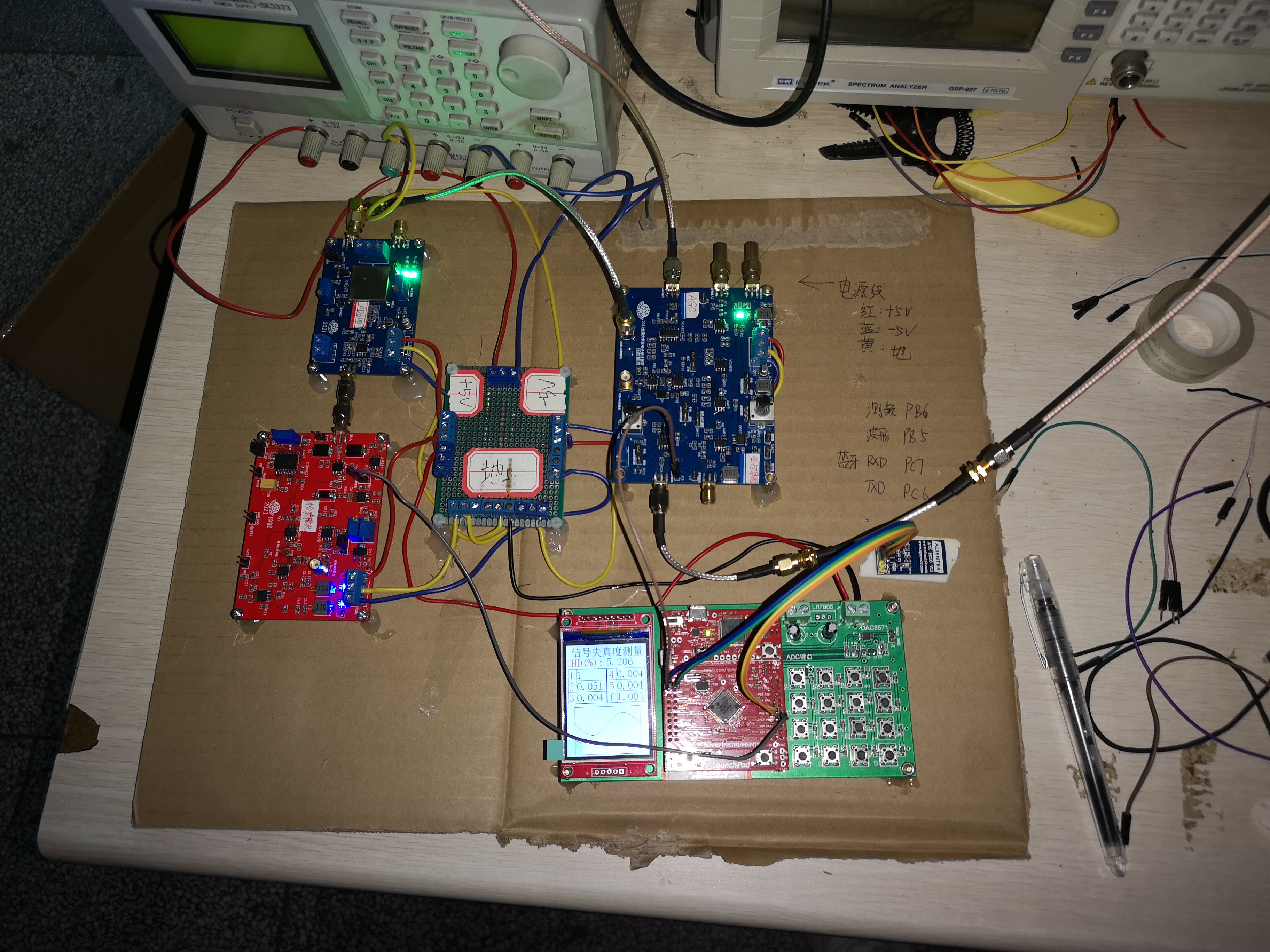
**Note: You also need to prepare a bipolar power supply and a smart Android phone. ** ## 9. Precautions
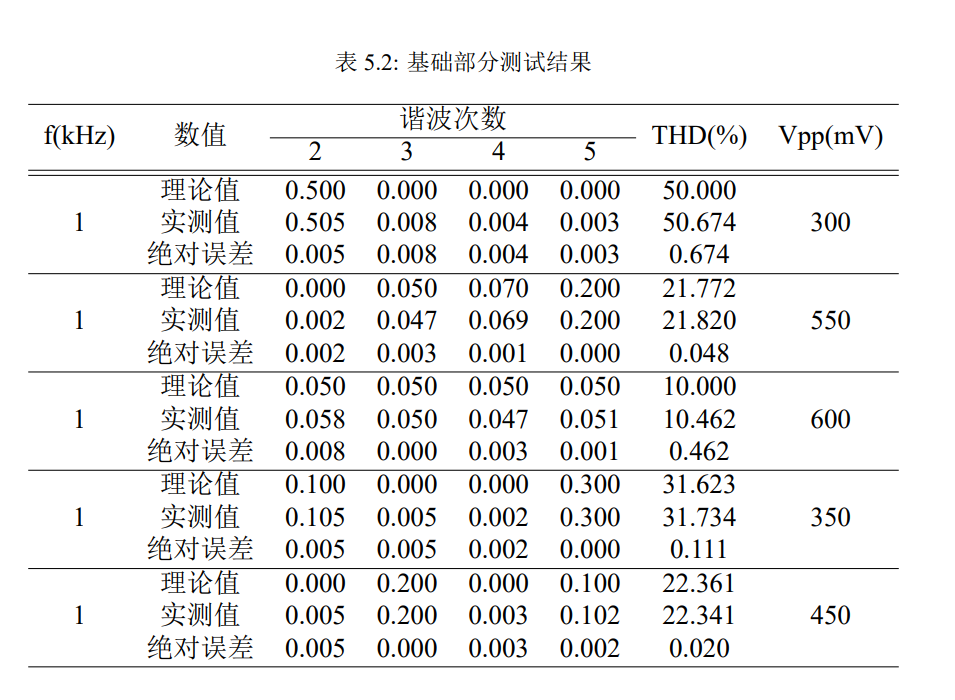
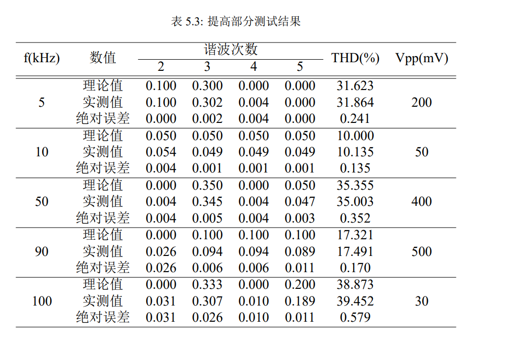
** Pay special attention to the input voltage limit of the ADC and protect it, otherwise the result will be in vain. ** ## 10. Test results
**Test plan**: Prepare ten sets of data, specify the normalized amplitude, frequency and peak-to-peak value of the four harmonics of each set of data, and use the signal source to output to the system , display data on the screen and conduct error analysis.
> Finished


 京公网安备 11010802033920号

 ADS820U


