Contents
1. Preface
2. Personal introduction
3. Project analysis
5. Theoretical analysis and calculation
6. Circuit analysis of each schematic diagram
7. Circuit pcb design analysis
8. Physical display
9. Program design
10. Summary
Preface
In the blink of an eye, electronic design among college students across the country The competition has come to an end, which also means that our electronic design journey this year has come to an end. Winning the first prize in the country is a reward for our four days and three nights, and it is also a reflection of our more than 200 days of serious preparation for the competition, but it is not enough to express our mood after the competition, not enough to represent our final harvest, not enough to make us happy. We stop moving forward. It is just a sign, and it is also a beginning. It marks that electronic design has been slightly understood, and it opens an extremely broad door to the electronic world.
Personal introduction : The topic
from the University of Electronic Science and Technology of China
requires

the project to analyze,
design and produce a wireless transceiver for mixed transmission of digital-analog signals on the same channel. Among them, the digital signal consists of a set of four numbers from 0 to 9; the analog signal is a voice signal with a frequency range of 100Hz to 5kHz. Wireless transmission is adopted, the carrier frequency range is 20~30MHz, the channel bandwidth is not greater than 25kHz, and the shortest transmission distance between sending and receiving equipment is not less than 100cm.
The transmitting end of the transceiver completes the combined processing of digital signals and analog signals, and then modulates and transmits them on the same channel. The receiving end of the transceiver completes reception demodulation and separates digital signals and analog signals. The digital signals are displayed with a digital tube and the analog signals are observed with an oscilloscope.
The task requires the design and production of a wireless transceiver for mixed transmission of digital-analog signals by the receiver. To achieve wireless transmission, reception, separation and decoding of signals, the overall system framework is shown in the figure.

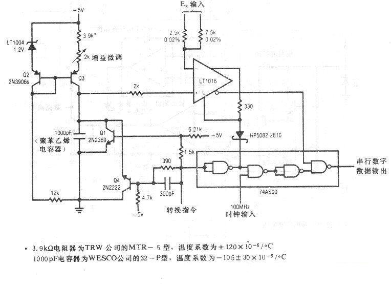
According to the topic requirements and scheme design, active RC filters are chosen to filter low-frequency signals. The advantage is that the design and production of the circuit are simple. The circuit diagram is as follows :

The mixing scheme uses multipliers to achieve performance comparable to passive mixers. And the loss is compensated with the help of gain, making the noise figure index better, thereby improving the overall linearity index of the receiver.
A major difficulty in this question is the separation of digital-analog signals by the receiver, so the demodulation scheme uses FPGA digital downconversion IQ demodulation. Its advantages are narrow demodulation bandwidth, strong selectivity, strong anti-interference ability and FIR can be used in this question. Filters separate digital and analog signals.
The transmitter amplification part uses low-noise amplifier PHA-13LN+ or TQP369182, both of which have extremely high dynamic range and low noise coefficient in a wide frequency range, as well as good input and output return losses. And the power supply voltage also has advantages in low power consumption. If TQP369182 is used as the main chip to build this circuit, the working cutoff frequency of the TQP369 amplifier circuit is determined by the inductor L1 and capacitors C2 and C3. These three components form a filter for frequency selection. The values of L1, C2 and C3 are selected according to the list:

From the above table, combined with the working requirements of the amplifier operating in the 25Mhz frequency band, L1, C2 and C3 can be appropriately increased. Select L1=1.8uH, C2=22uF, C3=22uF.
The local oscillator signal is generated by using the MCO pin of the low-power microcontroller STM32L431CCT6 to directly output the clock frequency set by the internal PLL. This solution consumes the lowest power and does not require redundant components.
Theoretical Analysis and Calculation
Since the question requires the channel bandwidth to be lower than 25kHz, FM modulation is used with a bandwidth BW=2*(Δf+fm) (where “fm” is the frequency of the modulated signal, and “Δf” is the maximum frequency deviation), and The required bandwidth for AM modulation is BW=2fm, so the AM modulation method that occupies a smaller channel bandwidth is selected.
Regarding bandwidth limitation requirements, the analog signal bandwidth is 50Hz to 10kHz, which has occupied the bandwidth of most AM modulated signals. Considering that digital modulation requires a response within 2s, the data to be transmitted is calculated according to four decimal digits,
which requires 14 bits . The binary bits, plus the three-digit frame header, total 17 bits (the response time does not include the frame tail). Select 10bit/s as the modulation rate of the digital signal. Theoretically, data can be sent once in 1.7s, and can be completed within the 2s required by the question. Digital transmission and reception.
For the modulation of the combined signal, in order to minimize the power consumption of the transmitter, a microcontroller is used to read the keyboard input and output the digital signal through the DAC. A simple adder is built through a resistor to add the analog signal αsin(wt) with The digital signal βA (θt) after the source RC filter outputs a combined digital and analog signal. The PLL inside the microcontroller is used to generate the local oscillator signal and the AD835 multiplier is used for AM modulation. Amplitude modulation uses the modulation signal to control the amplitude of the high-frequency carrier. , the process of making it change linearly with the modulation signal. The envelope of an AM signal is proportional to the modulating signal. In this solution, the combined signal of the addition output can be expressed as S(t)=αsin(wt)+βA(θt). The combined signal and the local oscillator signal cos(μt) of the microcontroller are input into the multiplier. The AM signal S_AM (t)=S(t) cos(μt) is obtained. It can further be obtained that the spectrum bandwidth of the AM signal is up to 20kHz, which meets the bandwidth limit requirements of the question.
The output filter is an LC filter, which should have an attenuation greater than 40dB at 48MHz (the second-order harmonic of the 24MHz local oscillator). The smaller the attenuation at 28MHz (the maximum local oscillator frequency), the better. The Filter solution simulation results are as follows:

Circuit analysis of each schematic diagram
1. Mixing circuit
In order to minimize the power consumption of the transmitter, the microcontroller DAC is used to output the digital signal and the local oscillator signal is output through the internal PLL. The digital signal is filtered by the active RC filter and then passes through the resistor network. It is directly added to the input audio signal to output a digital-analog combined signal. A multiplier is used to multiply the local oscillator signal and the combined signal for AM modulation. The AM transmitting circuit is composed of an AD835 as a multiplier for modulation. Compared with a passive mixer , although the multiplier produces a certain amount of power consumption, the input port has high linearity, and the input signal will not be distorted in phase and frequency due to device limitations. Moreover, the output combined interference signal is less. The positive and negative poles of the power supply part of the AD835 circuit are rectified using rectifier diodes respectively. According to the data sheet, 4.7uF tantalum capacitors and 0.01uF ceramic capacitors should be used for decoupling. The carrier frequency can reach up to 300MHz, which meets the requirements of this question. According to the internal circuit, the basic output relationship formula is:

the modulation signal is input from X. The X input range is ±1V, +U≈1.05V, and the modulation coefficient is determined by the resistors R6 and R7 between W and Z, or by changing the Y terminal. In this question, the XIN terminal can input the digital-analog combined signal, YIN can input the local oscillator signal, ZIN can be left empty, and W can output the mixed signal.

2. Amplification circuit
The amplification circuit consists of three parts: DC blocking, amplification, and frequency selection. The frequency selection part is adjusted according to the data sheet to obtain the best gain effect. The specific values can be found in the calculation part.

3. Overall circuit of the receiver
3.1 FPGA core board
The schematic diagram of the FPGA receiver core board can be found in the appendix, and the onboard program schematic diagram is as follows:
The FPGA receiver adopts a direct sampling + digital down-conversion IQ demodulation architecture. The front-end ADC acquisition rate is 65Msps (with a 30M low-pass LC filter and a 20db drive amplifier), with a 14-bit resolution. The high-speed parallelism of the ADC acquisition is obtained. After the data stream is IQ mixed with digital DDS, two digital signals are obtained. The digital signals are low-pass filtered. After step-by-step extraction, a digital baseband signal with a sampling rate of about 60k is obtained. High-pass and low-pass FIR filters are used to obtain analog signals. After demodulation, the digital baseband data is sent to the DAC to output a dual-channel analog digital waveform. The microcontroller then uses the ADC to collect the digital signal output for subsequent decoding processing. The microcontroller can also use the SPI protocol to change the phase increment control word of the DDS inside the FPGA. Thereby changing the local oscillator frequency.
When demodulating, the receiving end will demodulate the signal as an FM signal at the same time, thereby obtaining the deviation between the carrier wave and the local oscillator frequency, so as to conduct real-time frequency tracking. The microcontroller can also read the desired parameter value (carrier wave) through the 32-bit data register. Frequency and signal strength indication).

3.2 Receiver power supply circuit The
receiver power supply is mainly composed of two tps7A4701 chips. The circuit structure is as follows: it

can be purchased online or drawn directly according to the chip data manual. The overall structure is not difficult. Due to the time of the competition, a ready-made power supply is used. plate. In addition, because the lithium battery is used for power supply, the voltage drop is relatively large, so a small fan is used to dissipate heat from the chip.
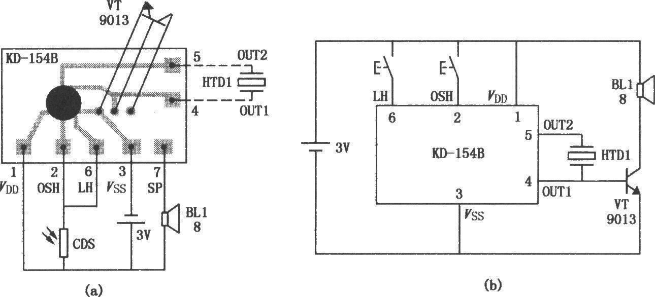
3.3 Digital tube circuit
Since the question requires four digital tubes, the circuit connection of the unit digital tube is more complicated and increases the time cost, so a four-digit integrated digital tube is used. The pin diagram is as follows:

Each pin is defined as
| a 11 | b 7 | c 4 | d 2 | e 1 | f 10 | g 5 |
| h 3 (decimal point pin) | C0 6 | C1 8 | C2 9 | C3 12 |
When the corresponding pin is connected to high level, it corresponds to a single light-emitting diode Lights up. For example, for the first common anode digital tube, if pin 12 is high level, 11, 7, 4, 2, 1, 10, 3 are low level, and 5 is high level, then the first The digital tube displays the character "0". However, each digital tube can only light up one digit at a time. To display a series of numbers on four digits, you need to use the dynamic scanning principle of the digital tube. That is, the four digital tubes light up quickly in sequence. Due to the visual residue of the human eye, It can achieve the effect of four digital tubes lighting up at the same time.
Circuit pcb design analysis
The wiring of high-frequency circuit boards requires the signal path to be as straight as possible to avoid the parasitic capacitance of high-frequency high-speed signals generated by the corner wiring. In addition, since the line width of the transmission line will change at the corner, the change of line width will also cause signal Reflection; holes can be drilled around the signal line for grounding to reduce the parasitic capacitance of the copper layer. For chips with high power supply voltage requirements, tantalum capacitors and ceramic capacitors need to be connected in parallel near the power supply port to decouple the power supply to make the power supply voltage ripple as small as possible. In addition, for signal interfaces, it is necessary to select an appropriate transmission line frame based on the impedance calculation tool and the number of board layers and thickness. For some special chips, the impedance line design needs to be based on the guidance of its data sheet.
Program design
1. Program flow chart

2. The main program display
can be downloaded in the attachment.
Physical display,

transmitter part,

receiver part,
summary.
After four days and three nights of hard work, our work has basically met all the requirements of the competition questions, and was completed on the last day. A successful digital transfer was achieved in the afternoon with just a few hours remaining before the game. In the subsequent evaluation, the full function of the work was also brought into play, and it achieved good evaluation results, and then won the first prize in the country. During these four days, we fully understood ourselves and felt tired and nervous with everyone. Sweat and joy accompanied us. After participating in the electronic design competition, we truly felt the challenges of life, felt the urgency of time, and learned to race against time.
Video link of the work https://www.bilibili.com/video/BV1SL411L77h?share_medium=android&share_plat=android&share_session_id=d1b21e9d-f555-48d6-a34a-7d0232a5e50d&share_source=QQ&share_tag=s_i×tamp=1639634615&unique_k=HIu Dj4I


 京公网安备 11010802033920号

 XC9110E181MR