## This project won the first prize in the 5th Electronic Design Competition of Zhejiang Sci-Tech University
#### Team number: ZSTU013
#### Team members: Wu Qingpeng, Sun Jing, Xie Zhouyang
#### Instructor: Jin Hai
## Design summary report of "School-level Electronic Design Competition"
### Abstract:
In some battery-powered devices, many of them obtain the required high voltage through DC boost circuits, such as the flash in a camera. This design requires converting the battery's electrical energy into a constant current output to drive a high-brightness white LED. The core part of the design is a DC-DC regulated current power converter, which realizes constant current output through a constant current control circuit after voltage conversion. Using STM32 as the controller, the output pulse is controlled, and a mode selection and alarm module consisting of independent buttons and buzzers is configured. The design circuit is mainly composed of a DC/DC voltage conversion module, a control module, a mode selection module, a constant current control module, a protection circuit module, and an alarm circuit module.
### 1. Project Tasks
* Design and make an LED flash power supply. The core of the power supply is a DC-DC current-stabilized power converter, which converts the battery's electrical energy into a constant current output to drive a high-brightness white LED. The power supply has two modes: continuous output and pulsating output, and has output voltage limiting protection and alarm functions.
##### 1. Basic requirements
(1) Input voltage 3.0V~3.6V.
(2) The output current in the continuous output mode can be set to three levels: 100, 150, and 200mA. The highest output voltage is not less than 10V, and the lowest output voltage is 0V (output short circuit).
(3) Within the specified input voltage and output voltage range, the relative error of the output current is less than 2%.
(4) When the equivalent DC load resistance is too large, the output voltage limit value is not higher than 10.5V and an alarm is issued.
(5) When the output current is 200mA and the output voltage is 10V, the efficiency is not less than 80%.
(6) Make a homemade LED flash light for demonstration.
##### 2. Performance part
(1) It has a pulsating output mode, the output duty cycle is 1/3, and the relative error is less than 2%.
(2) The output current peak can be set to 300, 450, and 600mA, the relative error is less than 5%, and the intermittent current is less than 1mA.
(3) The pulse period can be set to 10, 30, and 100ms, the relative error is less than 2%, the rise time and fall time are both no more than 100μs, and the current overshoot is no more than 10%.
(4) The number of output pulses can be set to 1 to 5 and continuous pulse trains (for testing), and a pulse train is output each time the start button is pressed.
(5) Others
### 2. Comparison and selection of solutions
##### 2.1 Overall system solution
The system is based on the STM32 microcontroller to form a DC/DC boost circuit, which provides a large voltage that meets the requirements for the output end. The constant current circuit is formed by INA282, so that the circuit can output a stable controlled current to meet the design accuracy requirements. The overvoltage detection circuit obtains the voltage difference between the two ends of the load and compares it with the reference voltage to output the overvoltage signal and transmit it back to the single-chip microcomputer. The system control module is designed based on the STM32 single-chip microcomputer, including keyboard circuit, buzzer alarm circuit, display circuit, mode selection circuit, constant current module, etc.
The system function block diagram is shown in Figure 1.

Figure 1 System function block diagram
##### 2.2 Power conversion module
* Option 1: Use TPS61088 boost chip to implement. TPS61008 is a fully integrated boost converter with high power density. Although it is efficient and can meet the design requirements, it is costly and therefore less used.
* Option 2: Build a BOOST DC boost circuit by yourself. The design parameters of each part of the circuit can be selected independently, with good adjustability and flexible design. However, due to limitations in component quality and accuracy, the functional stability is poor. After adding additional stabilization and protection circuits, the circuit efficiency is reduced.
* Option 3: Build a bidirectional DC-DC module, use the STM32 microcontroller to control the PWM wave duty cycle to control the output voltage of the circuit, and the microcontroller is simple to operate, has high precision, strong stability, high circuit efficiency, and requires few components and can provide stable voltage.
Based on the above analysis, this solution requires a boost module with low input voltage, high output voltage, high power, high precision, and high power efficiency, so option 3 is chosen.
##### 2.3 Constant current control circuit
* Option 1: Use a constant current diode. The advantage is that the circuit structure is simple, and the disadvantage is that the constant current characteristics of the constant current diode are not very good, the current specifications are relatively small, and the design accuracy requirements cannot be met.
* Option 2: Use two transistors of the same model and use the relatively stable be voltage of the transistor as a reference. This constant current source is simple and easy, but even the be voltage of transistors of the same model has individual differences, so it is not suitable for high-precision constant current requirements.
* Option 3: Use INA282 to convert the current of the circuit into a voltage signal, which is convenient for collection and feedback, and INA282 has a large amplification factor and stable operation.
Based on the above analysis, this design adopts Option 3.
### 3. Circuit Design
##### 3.1 Circuit Design of Single-Chip Microcomputer Function Module
This design uses STM32 single-chip microcomputer as the controller. In addition to the single-chip microcomputer minimum system, the input keyboard, display output, buzzer alarm circuit and other parts are built on the periphery. The output signal of the port is changed by key input to control and adjust the output current.
After receiving the overvoltage signal of the overvoltage detection module through the input port, the buzzer alarm is triggered to realize the alarm for the output voltage above 10.5V. The display output is completed by the LCD screen, which monitors the changes of some parameters in the circuit and displays them in real time. The input keyboard consists of 6 independent buttons, which are set as: mode selection button, current selection button, pulse cycle selection button, pulse number selection button, pulse trigger and close button.
The schematic diagram of the single-chip microcomputer function module is shown in Figure 2, and the button connection diagram is shown in Figure 3.

Figure 2 Schematic diagram of the microcontroller function module

Figure 3 Button connection diagram
##### 3.2 Boost module circuit design
This design uses a bidirectional DC-DC circuit for boosting. By controlling switches T1 and T2, the purpose of bidirectional DC boost and buck is achieved. When the boost operation is in progress, T2 is activated, T1 is turned off, and the converter works in the Boost state; when T1 is activated and T2 is turned off, the converter works in the Buck state to achieve the buck function.
This design only uses the Boost function of the circuit, but compared with the pure Boost circuit, it can improve the stability of the circuit. This design uses IR2103 as a signal amplifier chip to drive the switch tube to turn on to achieve boost. The
schematic diagram of the boost module circuit is shown in Figure 4.

Figure 4 Schematic diagram of the boost module circuit
##### 3.3 Constant current module design
This design uses INA282 as a constant current module. INA282 is connected to both ends of the sampling resistor. It can convert a small current signal into a voltage signal and amplify it, and transmit the voltage signal back to the microcontroller, and work together with the microcontroller to complete the constant current.
The schematic diagram of the constant current module circuit is shown in Figure 5.

Figure 5 Schematic diagram of constant current module circuit
##### 3.4 Overvoltage detection and alarm signal generation circuit
This design uses a voltage detection alarm with voltage division detection. A high-resistance resistor is connected in parallel at both ends of the load, and the ADC function of the microcontroller is used to collect and convert the voltage. When the voltage exceeds the voltage limit, an alarm signal is issued.
The alarm signal generation circuit uses a buzzer. When the detection voltage is too high, the microcontroller sends a high-level signal to control the transistor to conduct, and the buzzer sends an alarm sound.
The schematic diagram of the overvoltage detection and alarm signal generation circuit is shown in Figure 6.

Figure 6 Schematic diagram of overvoltage detection and alarm signal generation circuit
##### 3.5 The display circuit
uses TFTLCD as the display, which can display the current mode, current setting current, current setting cycle and current setting cycle number.
##### 3.6 The LED lamp circuit
uses the classic LED white light lamp as the load, with a rated power and rated voltage of 3V3W. Multiple series connection can meet the design requirements, with the characteristics of stable light emission and high brightness.
### 4. Programming
##### 1. MCU IO port pin assignment table
| | |
| --- | --- |
| IO port| Function|
| PA0 | Pulse trigger button|
| PA3 | Current selection button|
| PA12 | Mode selection button|
| PC6 | Pulse cycle selection button| | PC7
| Pulse number plus 1 button|
| PC8 | Pulse number minus 1 button|
| PA2 | Relay control|
| PD2 | Pulse control|
| PB5 | Alarm signal control|
| PA8 | PWM wave output|
| PC3 | Current feedback|
| PC1 | Load upper end voltage detection|
| PC0 | Load lower end voltage detection|
| PA13 | LCD_PWR |
| PA1 | LCD_RST |
| PA6 | LCD_DC |
| PC4 | LCD_CS |
| PA5 | SPI port|
| PA7 | SPI port|
Table 1 MCU IO port pin assignment table
##### 2. Program software flow chart
After the system is powered on, it enters the mode selection interface, and the microcontroller scans to realize key detection. Use the buttons to select continuous/pulsating output mode, output current, pulse period, and number of pulses. The microcontroller determines the output pulse timing through the timer and outputs the corresponding pulse control signal. At the same time, the overvoltage signal is cyclically detected in the main program. When there is an overvoltage signal input, the buzzer alarms.

Figure 7 Basic flow chart of program software
### V. Test plan
##### 5.1 Test instruments
| Serial number| Name|
| --- | --- | |
1 | Multimeter|
| 2 | Power supply|
| 3 | Oscilloscope|
| 4 | Sliding resistor|
Table 2 Test instrument table
##### 5.2 Test method
###### 5.2.1 Current test:
Connect a multimeter and a sliding resistor in series at the output end of the power supply, adjust the value of the sliding resistor, select the 100mA output, record the measured data, continuously adjust the sliding resistor and observe whether the current changes. Similarly, test the 150mA and 200mA current ranges.
###### 5.2.2 Efficiency test:
Connect a power supply platform and a multimeter in series to the power input of the LED flashlight, connect a sliding rheostat in series to the power output of the LED flashlight, and adjust the sliding rheostat to 50Ω. The calculation formula is:

###### 5.2.3 Pulse output test:
Connect an equivalent resistor to the output end, select the pulse output mode, set the cycle and determine the output, connect the oscilloscope ground terminal to the negative output end, and connect the oscilloscope probe to the positive output, observe the oscilloscope duty cycle, cycle, rise time, fall time and other data and record them.
### VI. System debugging
6.1 When the input voltage is 3V, select the circuit mode as "continuous output +100mA". Adjust the load size and measure the output current value to be around 100mA.
 
6.2 When the input voltage is 3V, select the circuit mode as "continuous output +200mA". Adjust the load size and measure the output current value to be around 200mA.
 
6.3 Select the circuit mode as "pulsating output + 300mA + period 10ms + continuous pulse train". Adjust the load size and measure the duty cycle to be 1/3, the period to be around 10ms, and the output current to be around 300mA.

### VII. Data testing and processing
7.1 Basic requirements Test
by connecting an external sliding resistor, continuously increase the load resistance at current values of 100mA, 150mA, and 200mA, and observe the changes in output current.
| Resistance (Ω) | Set Current (mA) | Measured Current (mA) | Error (%) | Efficiency|
| ----- | -------- | -------- | ----- | --- |
| 35.00 | 100 | 99.2 | 0.8 | |
| 150 | 148.4 | 1.066666667 | | |
| 200 | 199 | 0.5 | | |
| 40.00 | 100 | 98.7 | 1.3 | |
| 150 | 147.5 | 1.666666667 | | |
| 200 | 196.5 | 1.75 | | |
| 45.00 | 100 | 98.6 | 1.4 | |
| 150 | 147.5 | 1.666666667 | | |
| 200 | 198.5 | 0.75 | | |
| 50.00 | 100 | 98.6 | 1.4 | |
| 150 | 147.2 | 1.866666667 | | |
| 200 | 197.2 | 1.4 | 90.70% | |
Table 3 Data record (input voltage = 3V)
When the input voltage is 3V, the error between the recorded data and the ideal value is small, and each parameter meets the requirements of the question.
7.1.2 When the input voltage is 3.3V, the relevant parameters are recorded as follows.
| | | | | |
| --- | --- | --- | --- |
| Resistance (Ω) | Set current (mA) | Measured current (mA) | Error (%) | Efficiency |
| 35.00 | 100 | 99.3 | 0.7 | |
| 150 | 148.2 | 1.2 | | |
| 200 | 199.1 | 0.45 | | |
| 40.00 | 100 | 99.1 | 0.9 | |
| 150 | 147.6 | 1.6 | | |
| 200 | 198.2 | 0.9 | | |
| 45.00 | 100 | 98.7 | 1.3 | |
| 150 | 147.9 | 1.4 | | |
| 200 | 198.1 | 0.95 | | |
| 50.00 | 100 | 98.8 | 1.2 | |
| 150 | 147.3 | 1.8 | | |
| 200 | 198 | 1 | 92.20% | |
Table 4 Data record (input voltage = 3.3V)
When the input voltage is 3.3V, the error between the recorded data and the ideal value is small, and each parameter meets the requirements of the question.
7.1.3 When the input voltage is 3.6V, the relevant parameters are recorded as follows.
| | | | | |
| --- | --- | --- | --- |
| Resistance (Ω) | Set current (mA) | Measured current (mA) | Error (%) | Efficiency |
| 35.00 | 100 | 99.4 | 0.6 | |
| 150 | 147.9 | 1.4 | | |
| 200 | 199.3 | 0.35 | | |
| 40.00 | 100 | 98.8 | 1.2 | |
| 150 | 148.2 | 1.2 | | |
| 200 | 199.1 | 0.45 | | |
| 45.00 | 100 | 99 | 1 | |
| 150 | 148.3 | 1.133333333 | | |
| 200 | 198.8 | 0.6 | | |
| 50.00 | 100 | 99.1 | 0.9 | |
| 150 | 148.1 | 1.266666667 | | |
| 200 | 198.9 | 0.55 | 90.20% | |
Table 5 Data record (input voltage = 3.6V)
When the input voltage is 3.6V, the error between the recorded data and the ideal value is small, and each parameter meets the requirements of the question.
7.2 Performance test
| | | | | | | | | | |
| --- | --- | --- | --- | --- | --- | --- | --- |
Resistance (Ω) | Set current (mA) | Measured peak current (mA) | Set period (ms) | Actual high level time (ms) | Actual low level time (ms) | Actual period (ms) | Current error % | Period error % |
| 30 | 300 | 295 | 10 | 3.36 | 6.6 | 9.96 | 1.67 | 0.4 | |
30 | 9.9 | 20.1 | 30 |
0
| 20 | 450 | 451 | 10 | 3.32 | 6.6 | 9.92 | 0.22 | 0.8 | |
30 | 10 | 20 | 30 | 0 | | | |
| 100 | 33.2 | 66.4 | 99.6 | 0.4 | | | |
| | 600 | 572 | 10 | 3.4 | 6.6 | 10 | 4.67 | 0 |
| 30 | 10 | 20 | 30 | 0 | | | | |
| 100 | 32.4 | 67.6 | 100 | 0 | | | | |
Differences between the measured parameters and the ideal values in pulsation output mode The error between the two is small, and the parameters basically meet the requirements of the topic.
### 8. Summary
This design took two weeks, and the team members got a lot of training in the whole process. It is a test of whether our foundation is solid and whether we dare to be serious about the knowledge we have learned. In these two weeks, we have consolidated the knowledge we have learned before and learned more new knowledge, which has benefited us a lot. It is not enough to learn optics in vain
. People who study engineering should pay more attention to hands-on ability. In this task, there are many hands-on parts, not only the circuit, but also how to connect the various modules together to make the circuit more The simplicity and beautiful appearance make the performance of the work more superior and stable. These are all tests for us, but in the end we still overcame these difficulties and completed the task.
When we first learned about the topic, we conceived of multiple solutions and tried them one by one. In the end, the bidirectional DC-DC circuit we adopted was stable and easy to control, and its accuracy and efficiency also met the requirements. The solution was further optimized to adjust the most suitable output frequency of the PWM wave and further improve the boost efficiency to meet the requirements.
During the test, we encountered many problems. After discussion and searching online, we solved the difficulties one by one. However, there are still some shortcomings in the design.
The school competition is coming to an end. During this period, our group had arguments, laughter, and boredom. But in the end, we made a work that we did our best. This competition is a great achievement. It has improved our abilities in all aspects, further strengthened our understanding of power supply design, and also made us realize the importance of teamwork. We will continue to work hard, summarize our shortcomings, and improve our knowledge and skills.
### IX. References References
1. “LED Flash Power Supply” Zhao Xiaoying Anhui Mechanical and Electrical Vocational and Technical College Wuhu, Anhui 241000 China;
2. “Design of LED Flash Power Supply” Peng Wen Hunan Industrial Vocational and Technical College Changsha, Hunan 410000 China.
10. Appendix
A. Design circuit diagram (schematic diagram, PCB diagram)
(a) Schematic diagram

(b) PCB diagram

B. Program
```
#include "led.h"
#include "delay.h"
#include "sys.h"
#include "usart.h"
#include "tftlcd.h"
#include "spi.h"
#include
#include "timer.h"
#include "key.h"
#include "dac.h "
#include "adc.h"
#include "pwm.h"
#include "pwmplus.h"
vu8 key = 0;
u16 temp;
int kp = 10; //ratio
int e1 = 0; //current error
int u = 0; //increment
void run(u16 I,u16 Pe,u16 Pu ){
int i,j;
j=1 ;
LED0=0; //Relay off
if(Pu!=9999){
delay_ms(Pu*Pe);
}
else if(Pu==9999){
while(j){
key=KEY_Scan(0);
switch(key) {
case WKUP_PRES:
j=0;
break;
}
}
}
}
int main(void)
{
u16 mode\_flag,i\_flag,period\_flag,pulses\_flag;
u16 adcxI_T,adcxI,adcxU;
delay_init(); // Delay function initialization
NVIC\_PriorityGroupConfig(NVIC\_PriorityGroup\_2);// Set interrupt priority group 2
LED_Init(); //Initialize the hardware interface connected to the LED
KEY_Init();
LCD_Init(); //Initialize LCD
Adc_Init();
Dac1\_Init(); //DAC channel 1 initialization TIM1\_PWM\_Init(7199,0);//72000000/7200=10khz
// TIM3\_PWM\_Init(7199,999);//72000000/7200/1000=10;//pe=100 a=999 pe=30 a=299 pe=10 a=99
uart_init(9600); //9600
TIM1->CCR1=4390;//Constant voltage module//100 4390 //150 2790 //
mode_flag=1;
i_flag=100;
period_flag=0;
pulses_flag=0;
LED2=0; //Buzzer off//B5
LED1=0; //Pulse off//D2
LED0=1;//Relay is turned on //A2
while(1)
{
adcxU=Get\_Adc\_Average(ADC\_Channel\_11,50);//Output voltage c1 upper end adcxI\_T=Get\_Adc\_Average(ADC\_Channel\_10,50);//Voltage at both ends c0 //Lower end adcxI=Get\_Adc\_Average(ADC\_Channel\_13,50);//Detection voltage, C3 LCD_ShowString(0, 0, 64, 32, 32,"mode");//Mode
LCD_ShowString(0, 40, 64, 32, 32,"i");//Current
LCD_ShowString(0, 80, 64, 32, 32,"peri");//Period
LCD_ShowString(0, 120, 64, 32, 32,"puls");//Number of pulses
LCD\_ShowxNum(80, 0,mode\_flag,8, 32, 0);
LCD\_ShowxNum(80, 40,i\_flag,8, 32, 0);
LCD\_ShowxNum(80, 80,period\_flag,8, 32, 0);
(80, 120,pulses\_flag,8, 32, 0);
LCD_ShowxNum(0, 160,adcxU,4, 32, 0);
LCD\_ShowxNum(80, 160,adcxI\_T,4, 32, 0);
LCD_ShowxNum(0, 200,adcxI,4, 32, 0);
LCD_ ShowxNum(80, 200,TIM1->CCR1,4, 32, 0);
key=KEY_Scan(0);
switch(key)
{
case KEY0\_PRES: //A12//Mode selection if(mode\_flag==1) {
mode_flag=2;
i_flag=300;
period_flag=10;
pulses_flag=1;
}
else if(mode_flag==2){
mode_flag=1;
g=100;
period_flag=0;
pulses_flag=0;
}
break;
case KEY1\_PRES: //A3//Current selection if(mode\_flag==1){
if(i\_flag==100) i\_flag=150;
else if(i\_flag==150) i\_flag=200;
else if(i\_flag==200) i\_flag=100;
}
else if(mode_flag==2){
if(i\_flag==300) i\_flag=450;
else if(i\_flag==450) i\_flag=600;
else if(i\_flag==600) i\_flag=300;
}
break;
case WKUP_PRES: //A0//Trigger pulse
if(mode_flag==2)
{
LED0=0; //Relay turns off
TIM3\ _PWM\_Init(7199,period\_flag*10-1);//72000000/7200=10000;//pe=100 a=999 pe=30 a=299 pe=10 a=99
TIM3->CCR4=2400;
run(i\_flag,period\_flag,pulses\_flag);
TIM_CtrlPWMOutputs(TIM3,DISABLE);
LED0=1; /Relay on
}
break;
case KEY2_PRES: //C6//Pulse period selection
if(mode_flag==2){
if(period\_flag==10.0) period\_flag=30.0;
else if(period\_flag==30.0) period\_flag=100.0;
else if(period\_flag==100.0) period\_flag=10.0;
}
break;
case KEY3_PRES: //C7//Pulse quantity selection plus
if(mode_flag==2){
pulses_flag++;
if(pulses\_flag==6) pulses\_flag=9999;
else if(pulses\_flag==10000) pulses\_flag=1;
}
break;
case KEY4_PRES://C8//Pulse number selection minus }if(TIM1->CCR1>=7000) TIM1->CCR1=4390;if(TIM1->CCR1C CR1=4390;TIM1->CCR1 +=u;u = 1 *e1;e1 = adcxI -2283;}TIM1->CCR1+=5;if(adcxI>2286){}if(TIM1->CCR1>=7000) TIM1->CCR1=4390;if(TIM1->CCR1CCR1=4390;if(adcxICCR1-=5;else if(i_flag==450){}if(TIM1->CCR1>=7000) TIM1->CCR1=4390;if(TIM1->CCR1CCR1=4390;TIM1->CCR1 +=u;u = 1 *e1;e1 = adcxI -1467;}TIM1->CCR1+=5;if(adcxI>1469){}if(TIM1->CCR1>=7000) TIM1->CCR1=4390;if(TIM1->CCR1CCR1=4390;if(adcxICCR1-=5;else if(i_flag==300){}if(TIM1->CCR1>=7000) TIM1->CCR1=4390;if(TIM1->CCR1CCR 1=4390;TIM1->CCR1 +=u;u = 1 *e1;e1 = adcxI - 968;}TIM1->CCR1+=5;if(adcxI>971){}if(TIM1->CCR1>=7000) TIM1->CCR1=4390;if(TIM1->CCR1CCR1=4390;if(adcxICCR1-=5 ;else if(i_flag==200){}if(TIM1->CCR1>=7000) TIM1->CCR1=4390;if(TIM1->CCR1CCR1=4390;>CCR1 +=u;u = 1 *e1;e1 = adcxI - 705;}TIM1->CCR1+=5;if(adcxI> 708){}if(TIM1->CCR1>=7000) TIM1->CCR1=4390;if(TIM1->CCR1CCR1=4390;if(adcxICCR1-=5;else if(i_flag==150){ }if(TIM1->CCR1>=7000) TIM1->CCR1=4390;if(TIM1->CCR1CCR 1=4390;TIM1->CCR1 +=u;u = 1 *e1;e1 = adcxI - 450;}}TIM1->CCR1 += 5;{else if (adcxI>454)}if(TIM1->CCR1>=7000) TIM1->CCR1=4390;if(adcxI>448 && adcxICCR1CCR1=4390;{(i_flag==100)//Current controlif}LED2=0;}else{TIM1->CCR1=4390;delay_ms (1000);; //B5 alarm);LED2=1delay_ms (1000);LED2=0; //B5 alarmdelay_ms (1000);LED2=1; //B5 alarmif(adcxU-adcxI_T>2126){//¾¯±¨}break;}else if(pulses\_flag==9998) pulses\_flag=5;if(pulses\_flag==0) pulses\_flag=9999;pulses_flag--;
if(mode_flag==2){
else if(i_flag==600){
if(adcxICCR1-=5;
if(TIM1->CCR1CCR1=4390;
if(TIM1->CCR1>=7000) TIM1->CCR1=4390;
}
if(adcxI>2926){
TIM1->CCR1+=5;
}
e1 = adcxI -2923;
u = 1 *e1;
TIM1->CCR1 +=u;
if(TIM1->CCR1CCR1=4390;
if(TIM1->CCR1>=7000) TIM1->CCR1=4390;
}
}
}
```
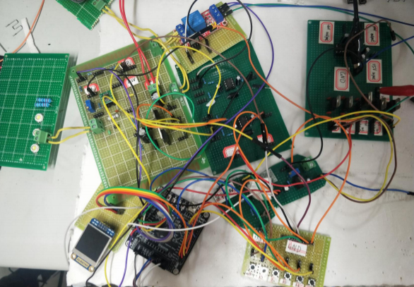
C. 作品图片


 京公网安备 11010802033920号

 MAX6381XS32D4-T


