This project is a pet drying box based on the STM32F103C8T6 microcontroller, featuring timer and automatic drying functions.
uses the STM32F103C8T6 microcontroller as the main controller, outputting PWM to control the on/off state of the SSR solid-state relay. The heating power of the PTC heating plate is controlled by changing the PWM duty cycle. A DHT20 temperature and humidity sensor monitors the temperature and humidity inside the drying box. An NTC thermistor can also be added for supplementary temperature measurement. An air duct is designed inside the pet drying box; it only needs to maintain the blown hot air at the set temperature, not the internal temperature. Multiple axial fans blow hot air to dry the pet. PID temperature control is implemented to ensure temperature stability. The PID strategy here is to ensure temperature stability and prevent overshoot, which can sacrifice some heating time; the temperature can only be low, not high. The on/off time of the SSR solid-state relay
is 10ms, therefore the PWM period for controlling the SSR solid-state relay is set to 20ms. The advantages of SSR solid-state relays include long lifespan, high reliability, high sensitivity, low control power, good electromagnetic compatibility, and fast switching. However, their disadvantages include large voltage drop after conduction, leakage current after semiconductor device turn-off, sensitivity to overload, influence of ambient temperature on load capacity, and higher cost. Note that the load terminal of the SSR solid-state relay must not be short-circuited; a short circuit will burn it out. Major online shopping platforms offer discounts for new users on SSR solid-state relays, making them available for as low as 1 to 3 yuan.
Controlling an axial fan involves using a microcontroller to output PWM to control the on/off state of a high-power MOSFET, thereby controlling the fan speed. The PWM control for the fan uses a MOSFET switching driver module with a maximum frequency of 20kHz. High-power MOSFET-triggered switching driver modules offer advantages such as fast switching, high efficiency, and simple control; however, they also have disadvantages such as high cost, complex driving, and sensitivity to external interference.
Both PWM control methods used above are heat-sensitive, but in this system, the operating power is low and the ambient temperature is not high. As long as it is not used directly on a PTC heating element, it is more than sufficient for this system.
The 0.96 OLED screen uses a 7-pin SPI interface; an 8-pin version is also available. Converting to a 4-pin interface is very simple; just replace the driver file.
The STM32F103C8T6 minimum system board in this system comes from the JLCPCB DiKuoXing open-source project. It is strongly recommended that those who are replicating this system purchase this ready-made minimum system board. Simply plug it into the corresponding pins. Hand-soldering double-sided boards with 0402 components is troublesome and prone to problems. The STM32F103C8T6 chip on the LCPCB website costs around 8 yuan, while the DiKuoXing ready-made board costs only 10.91 yuan. Alternatively, a domestic 32-bit development board, such as the DiWenXing CW32, can be used, which has excellent performance and stable operation.
This project involves 220V AC power. Always disconnect the power before modifying any circuit. Exposed terminals of the SSR solid-state relay should be insulated with silicone rubber or similar materials.
The upper left corner displays the temperature measured by a thermistor; currently, the code only shows this data, not used for temperature control.
Power-on starts temperature adjustment, default 39°C. The rotary encoder adjusts the temperature in 1-degree increments, up to a maximum of 60°C. Humidity data is displayed on the right. When exiting the temperature setting, the temperature and humidity sensor readings are displayed. Heating begins when the timer is not 0.
Pressing button 1 for the first time switches to fan speed adjustment; the default is 0, and the fan will rotate as long as it is not 0.
Pressing button 2 switches to time adjustment; heating begins when the time is not 0. Pressing button 2 switches to seconds, minutes, and hours, adjusted by the rotary encoder. Pressing
button 1 a third time switches to automatic mode, sets the temperature to 39 degrees Celsius, and uses the rotary encoder to adjust the on/off state. The idea is to automatically stop based on humidity data, but the humidity data fluctuates significantly, requiring further testing to confirm its feasibility (code not yet written). Currently, the temperature is set to 39 degrees Celsius, the fan is at 90% capacity, and it runs continuously.
Pressing button a fourth time returns to the first state.
, feel free to use your imagination to design the air ducts, etc. This project uses old wooden strips as the frame and thin wooden boards for the air ducts, resulting in lower costs. Aluminum profiles can also be used for the frame. It can be used as a pet cage for everyday use or designed as simple furniture.
As mentioned in the video, the entire unit can be made into a large cage; the fan has a thick filter that won't harm the pet, eliminating the need for a separate inner cage.
shows a box of newborn puppies.
The voltage and current meter designed based on ESP32S3 can measure voltage from 0 to 30V and current from 0 to 3A. It can be powered by a power input of 5 to 12V and can achieve a sampling rate of 0 to 10KHz. The voltage range is divided into two ranges: 0 to 6V and 0 to 30V.
For the sake of aesthetics and neatness when using color silkscreen printing, I will use surface-mount components as much as possible in the voltmeter and ammeter hardware design . At the same time, for ease of soldering, the component package size will not be smaller than 0603.
(The document content is the same as the attached "Voltmeter and Ammeter Hardware Design.docx". I first organized it in Word and then uploaded it, so the content is identical. You can view it offline after downloading, and you can directly correct any errors. It would be best if you could remind me of any errors.)
I. Chip Selection
This project requires the use of the LCSC development board. Considering the development difficulty and convenience, I chose the LCSC ESP32 board as the main controller. The following analysis is based on this board.
1.1 Power Supply Chip Selection
In terms of power supply, since the ESP32 board already has its own 5V power supply and a 3.3V conversion LDO circuit, we can directly choose to use the power supply on the board.
At the same time, I also plan to use a 9V battery as another power supply solution, so I also plan to make an input voltage regulator circuit for the power supply.
Since the board has a built-in 5V to 3.3V voltage regulator circuit, we only need to use one chip to regulate the input voltage to 5V.

Figure 1-1 shows the schematic diagram of the LCKFB-ESP32S3 power supply circuit
. For this requirement, we commonly use two types of chips: DC-DC and LDO.
Common LDO chips include the 1117 and 7805; here, I chose the SE8550K2, the same as in the tutorial. The 1117 has a lower maximum input voltage, is often counterfeited and difficult to obtain genuine copies, and requires tantalum capacitors, increasing the complexity and price of components, making it unsuitable for small-scale purchases and use.
(LDO is also called a series linear regulator because the input and output currents are equal; when the output voltage difference is large, the remaining energy is dissipated by the regulator circuit in the form of resistance.)
Regarding the DC-DC solution, due to the more complex external circuitry, it has a larger output ripple (more accurately, it has the property of output ripple, but this is easier to understand), and the chip price is also higher, so we do not choose it here. If you want to try it, the videos by Bilibili up-master "Engineering Man Sun" are excellent; you can refer to them for your production. Video BV number: BV1Mb4y127e9.
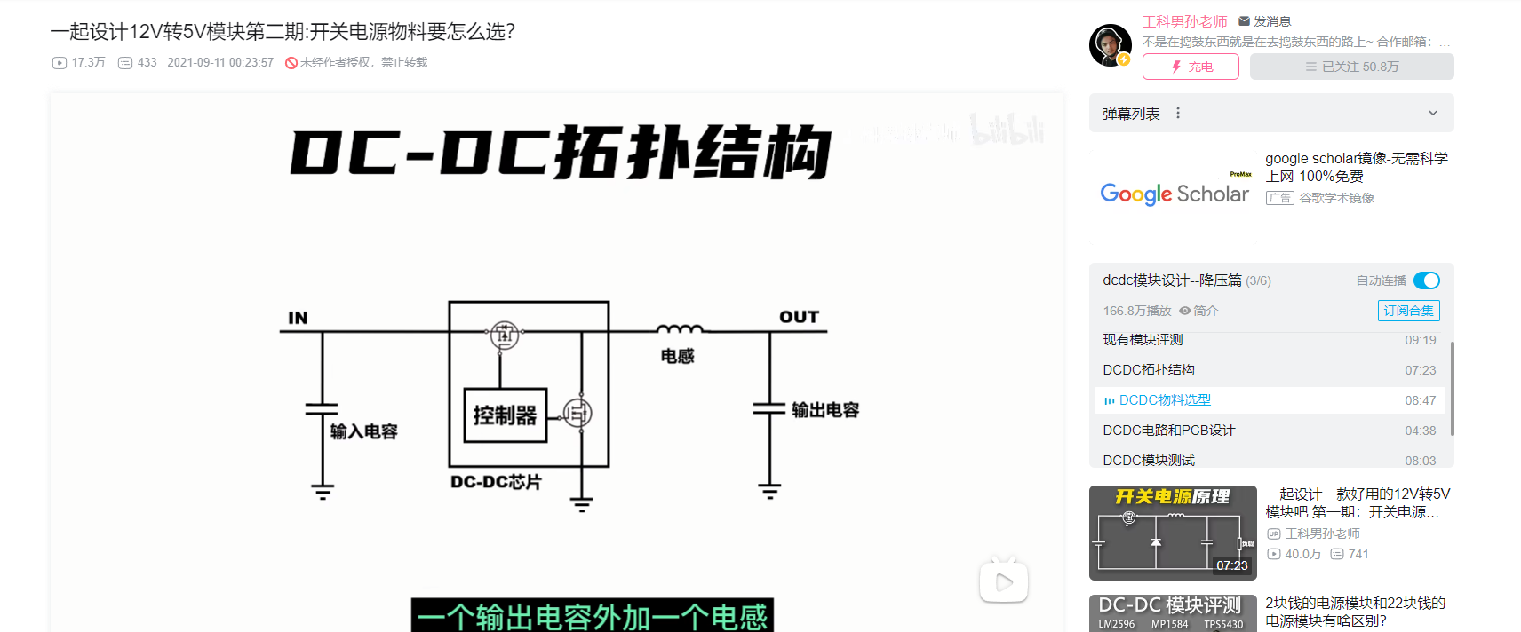
Figure 1-2 DC-DC Circuit Design Reference
1.2 Voltage Sampling
Voltage sampling We directly read the external input voltage using the board's ADC. If the sampling rate requirement is not high, the built-in ADC of the board can be used directly. Basically, the built-in ADCs of microcontrollers such as STM32, CW32, and TM4C are successive approximation type, so there's no need to be picky about this solution, and the speed is generally not high. Of course, it can still meet the requirements for audio signal spectrum analysis. (Performance-wise, it's not as good as CW32; choose freely according to your needs.)
Below are the electrical characteristics of the ADC module from the chip's datasheet. We chose the 0~1100mV range as a design reference, and the subsequent component parameters are calculated based on this value. Later, based on the actual error obtained from specific debugging, we will determine the final range and actual component parameters.
(LSB (Least Significant Bit) refers to the least significant bit, which corresponds to the resolution of the ADC. An 8-bit ADC with a reference of 5.12V has a resolution of 0.02V. When used to measure a voltage signal, a result of 100 means that the measured voltage value is 100 * 0.02V = 2V. Assuming its INL is 1LSB, this means that the true accurate value of the voltage signal is between 1.98V and 2.02V. Ideally, the corresponding number should be 99 to 101. The measurement error is one least significant bit, i.e., 1LSB. ----From reference link)
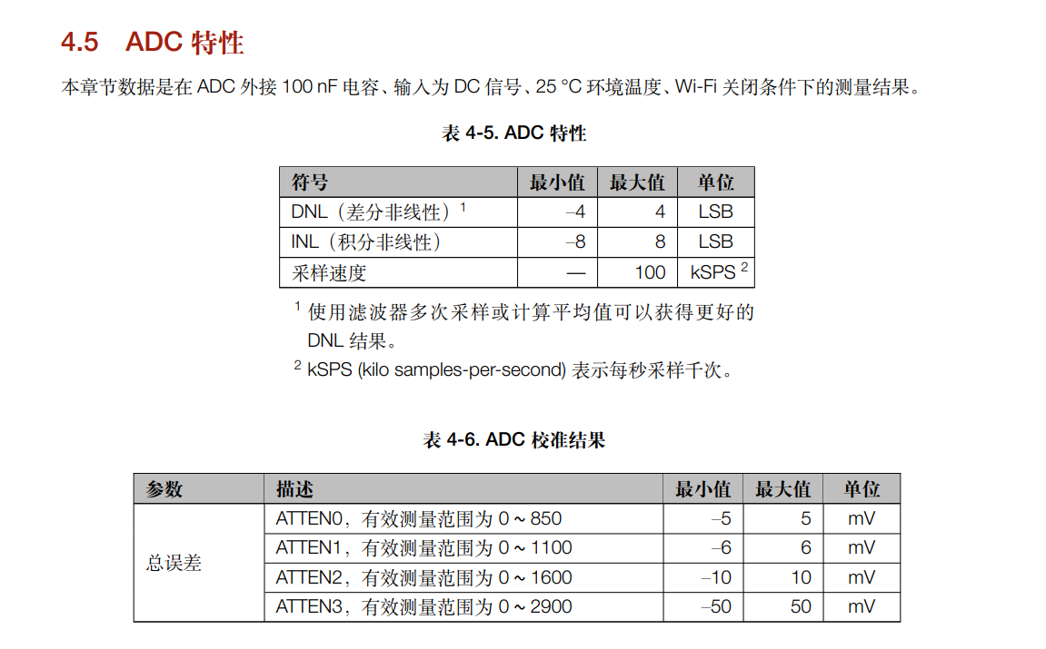
Figure 1-3 shows an example project in the electrical section of the ADC chip manual,
where a potentiometer is used to connect the power supply voltage to simulate the input voltage. Here, I intend to achieve higher integration, so I will not include this circuit on the board but will build it directly in the external circuit. I chose a DC-DC boost module for input measurement.
1.3 Current Sampling and Amplification
Principle: A sampling resistor is connected in series in the circuit, and the voltage difference across its two ends is measured to calculate the current.
Current sampling comes in two forms: high-side sampling and low-side sampling. We've brought out both positive and negative interfaces, allowing us to use either approach. This example uses low-side sampling, where the bottom side of the sampling circuit needs to share a common ground with the development board.
The example uses a 100mΩ resistor; considering contact resistance when connecting external circuits, a smaller resistor isn't necessary. For later testing, we can choose a larger voltage and resistor. Here, I plan to use a smaller resistor for amplification via a current sensing amplifier chip, preparing for circuits sensitive to input resistance.
Referring to another example (the last link; related content can be viewed through the link), I chose the INA199 chip for the current sensing amplifier. By consulting the datasheet, we can see that this chip has three amplification specifications. Since the current we're measuring isn't that small, and the sensitivity requirement isn't that high, we'll choose 50x, i.e., the INA199X1 series. We'll need to consider this amplification factor when designing components in the circuit later.
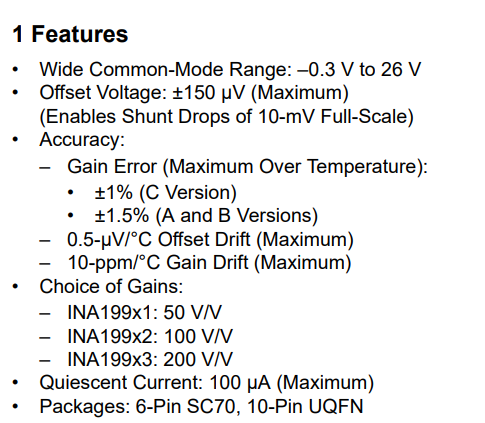
Figure 1-4 INA199 Chip Manual
1.4 Connectors
The connectors we use here are:
a standard female header for connecting the development board and the screen; and
a DC female connector for power input.
II. Schematic Design
2.1 Power Supply Circuit
The baseboard uses an SE8550K2 chip to regulate a 9V~12V voltage to 5V.
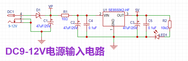
Figure 2-1 DC 9-12V Power Input Circuit
The following is a detailed description of this circuit:
1. A DC power socket is used as the input interface, accepting 9~12V voltage. In actual operation, it can accept 5~30V voltage, but the voltage rating and package of the electrolytic capacitors need to be adjusted.
2. A Schottky diode, D1, is connected in series in the forward direction to prevent reverse connection. When a reverse input voltage is applied, the resistance of D1 tends to infinity, preventing damage to the downstream circuitry.
3. R1 performs a voltage divider operation, reducing the problem of excessive heat generation caused by the large voltage difference of the LDO under high voltage conditions. On the other hand, utilizing the principle of low overcurrent of a series-connected 10-ohm low-power resistor, it acts as a low-resistance fuse, providing overcurrent or short-circuit protection.
4. Electrolytic capacitor C1 filters low-frequency ripple at the DC input, electrolytic capacitor C2 filters low-frequency ripple at the chip input, and electrolytic capacitor C3 filters low-frequency ripple at the chip output. When the input voltage is insufficient, it provides energy to the load. The capacitance values here are the same as the previously used electrolytic capacitors to reduce the type of electrolytic capacitors purchased. C4 and C5 filter the corresponding high-frequency ripple.
(When electrolytic and ceramic capacitors are used in parallel, the electrolytic capacitors first filter out the low-frequency portion of the input voltage, providing a stable DC voltage for the circuit. Subsequently, the ceramic capacitors further compensate for high-frequency fluctuations, filtering out high-frequency noise and pulse hazards. This high-low combination filtering method can more effectively filter out noise and fluctuations across the entire frequency band, improving the overall performance of the circuit. In addition, ceramic capacitors can eliminate the inductive characteristics (parasitic inductance of the capacitor) generated by electrolytic capacitors at high frequencies, further improving the filtering effect.)
5. R2 and LED1 form an indicator circuit, which can visually indicate the circuit's operating status.
2.2 Voltage Sampling Circuit
Here, our input voltage range is 0~30V, and our maximum sampling voltage is set to 1.1V. Therefore, the required resistor ratio is approximately 1:27. For ease of purchase, we choose a 300K resistor and a 10K resistor in series for voltage division. There is also a small voltage fine measurement circuit. (
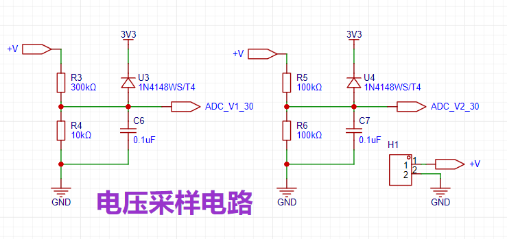
Figure 2-2 Voltage Sampling Circuit)
We also need to note that the maximum input voltage at the pin must be less than or equal to 3.3V. Therefore, we use a clamping diode to clamp the power supply to the 3.3V output on the board. The diode used is a switching diode, which can turn on quickly enough to protect the circuit.
Additionally, the chip design manual recommends adding a 100nF capacitor next to the ADC input pin for stability. Here, we place it next to the pin on the baseboard; its effect may be limited. This can be observed during subsequent actual measurements. Note that the 0.1uF capacitor should be placed next to the pin on the development board.
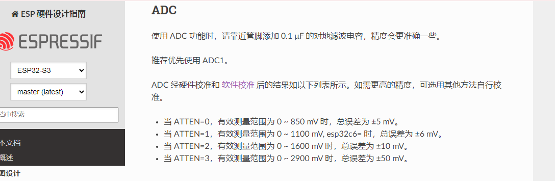
Figure 2-3 Hardware Design Guide Recommendation
2.3 Current Sampling and Amplification Circuit
Here we assume the highest sampling voltage is 1.1V. The maximum sampleable voltage before chip amplification is 22mV. Dividing by the highest input of 3A, we can get the corresponding sampling resistor as 7.3mΩ. Here we choose a 5mΩ sampling resistor for easy purchase.
Through this sampling resistor, we can calculate the corresponding current from the obtained sampling value.
That is: Sample value / 4095 * 22 (mV) / 5 (mΩ) = Corresponding current value (A)
By consulting the chip datasheet, we can find the basic circuit of INA199. (Typical Application of INA199)
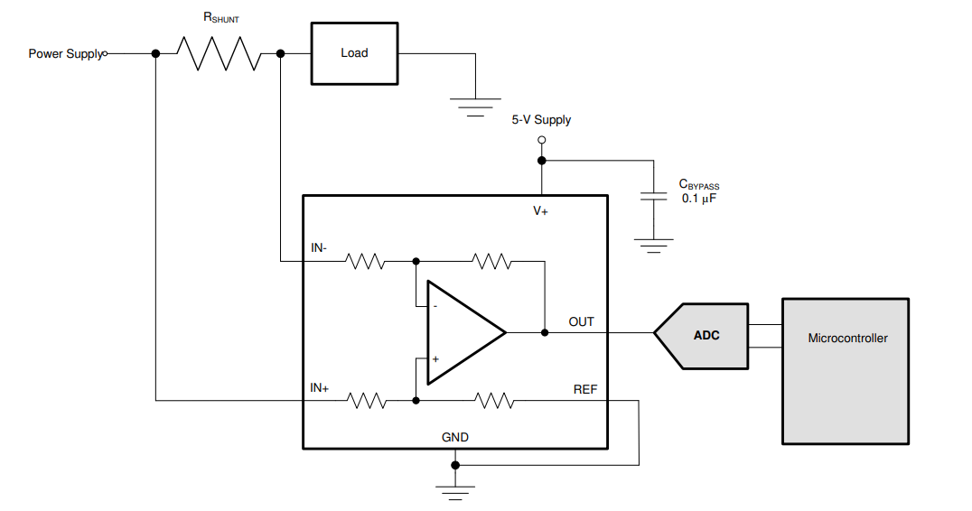
Figure 2-4 Typical Application of INA199
The current sampling circuit drawn with reference to this circuit is as follows.
Among them, R7 is the alloy sampling resistor, U5 is the current sensing amplifier chip, C8 is placed with reference to the above circuit, presumably a capacitor for power input filtering, so it will be placed close to the power pin, and C9 is a capacitor for ADC sampling filtering, so it needs to be placed close to the development board pin.
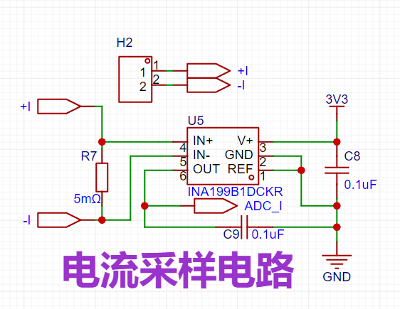
Figure 2-5 Current Sampling Circuit
2.4 Test Circuit
The left side shows the input signal, and the right side shows the corresponding pins and test points. This allows for testing during operation. Here, the package of the test points needs to be changed to match the package of the components used later.
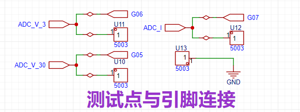
Figure 2-6 Test Point and Pin Connection
Here, copper lead plates purchased from Taobao are used because they are inexpensive and meet the requirements (I used a 2 yuan coupon; without the coupon, the actual purchase would be 2 yuan more expensive). The purchased package is 2*3, so we need to change the package diameter to 2mm. The overall diameter can then be set according to actual needs; here, I set it to 2.7mm. (I didn't actually use this in practice; I found that I could directly plug in a voltmeter for testing.)
Taobao link: https://item.taobao.com/item.htm?id=522092049395

Figure 2-7 Copper Chicken Leg Purchase
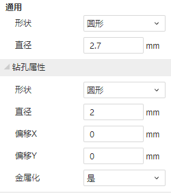
Figure 2-8 Test Point Package Attributes
2.5 Other Peripherals
In the first version, I put four buttons, but I felt they weren't very user-friendly, so in the second version, I added two rotary encoders. I plan to write a low-sampling-rate oscilloscope mode in the software; the knobs on the oscilloscope are indeed more convenient.
To coordinate well with the subsequent silkscreen printing, the rotary encoders are placed in the following two positions:
At the same time, some space is reserved to prepare for adding other functions later.
Also, in the second version, I placed the power supply section on the left side, with separate copper plating, to provide some isolation.
III. Hardware Soldering and Testing
3.1 Soldering and Testing Sequence
During the soldering process, I first soldered the power supply section, using solder paste and a hot air gun to solder it on in one go. Note that after using the hot air gun, remember to check for short circuits in the power supply section (5V and GND, as well as the diode terminals and GND). The capacitors on the board have small capacitance values, so it's not a big deal if they explode. However, if the power input is short-circuited and there is no short-circuit protection at the input (most chargers should have this), it could damage a low-quality charger.
Next, I soldered the voltage sampling circuit, which can be tested directly without a power supply.
Then I soldered the current sampling circuit, which requires connection to the core board to operate because the 3V3 power supply used by the chip is only available on the core board.
Finally, I soldered the remaining parts in the order of RF connector, header, and rotary encoder.
3.2 Soldering Precautions
Before soldering the voltage sampling circuit, remember to use a multimeter to test the following components to facilitate more accurate voltage estimation based on the specific resistance values later.
During the soldering process of the current sampling circuit, we need to pay attention to the direction of the silkscreen of the current sensing amplifier chip, because it is relatively small. The silkscreen shape and specific pin definition in the software are shown in
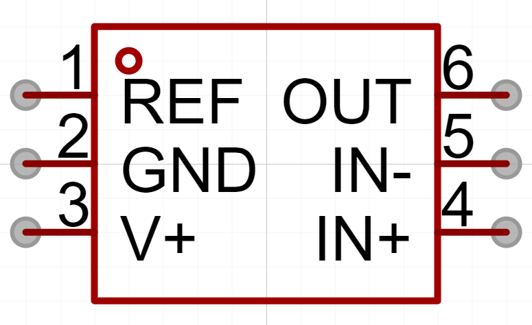
Figure 3-1: Component shape in PCB design
. The silkscreen of the chip itself is shown in

Figure 3-2: Chip silkscreen .
Through these, we can roughly infer that the orientation of the dotted silkscreen is the same as the horizontal line on the chip, but it is not accurate. Therefore, we need to find the corresponding pin definition in the chip datasheet and compare it with the pin on the PCB.

Figure 3-2: Chip datasheet pin definition
. Here, through the comparison of the pins, we can find that the horizontal line is indeed in the same direction as the dot.
At the same time, when soldering this chip, due to its small pin spacing, it is easy to bridging. Remember to test whether there is bridging between the following two pins after soldering (only use a multimeter in continuity mode to connect between the two pins). Also, since pin 1 (REF) and pin 2 (GND) are both connected to ground, they are connected to each other.
3.3 Circuit test content
1. Power supply circuit: After measuring according to the description in the soldering test sequence, power on. If LED1 lights up normally, it indicates that the circuit is functioning correctly.
2. Voltage sampling circuit: Before soldering, measure the resistance values and calculate the voltage at the test point based on the specific resistance ratios. Compare this
calculated voltage with the actual measured voltage value. The measured resistance values of the four resistors are: R3 - 300.4K, R4 - 9.96K, R5 - 100.1, R6 - 100.8K.
Therefore, we can calculate that in the 0~30V sampling range, the voltage at the test point = input voltage * 9.96 / (9.96 + 300.4). In the 0~3V sampling range, the voltage at the test point = input voltage * 100.8 / (100.8 + 100.1).
This voltage test uses a boost module powered via Type-C. We can easily draw 5V from the input terminals for the current sampling circuit and 5~30V from the output terminals for the voltage sampling circuit.

Figure 3-3 Boost Module
3. Current sampling circuit: After soldering, first test the pin bridging of the current sensing amplifier chip. After passing the test, test the continuity between GND and the 3V3 and 5V networks to prevent short circuits from damaging the core board. This is because the chip requires the 3V3 power supply from the core board for this test.
Then measure the output power supply of the boost module (or directly use its input power supply) and record its value (e.g., 9.241V during the test). Then calculate the appropriate resistance value based on the power and current (100 ohms were used in the test; if the supply voltage is lower, the resistance can be lower, the current can be larger, and the test current range can be larger).
Through calculation, we can obtain that the output voltage should be equal to: Input voltage / Circuit impedance * Sampling resistor impedance * Sensing amplification factor = 9.241 / 100 * 0.005 * 50 = 0.231V.
The following are the actual measurement results:

Figure 3-4 Current sampling module test results.
It can be seen that the result differs from the calculated result by about 0.02V, which translates to a measured current of 80mA. This is not the maximum measurement error, but it can provide some reference.
3.4 Module Testing
1. TFT Screen Test
Insert the development board into the corresponding socket as shown in the figure, and insert the TFT screen into the corresponding socket as shown in the figure. Connect it to the computer via the Type-C interface.

Figure 3-5 Connection Diagram
Compile and burn the "TFT_TEST.ino" file, and observe whether the TFT screen displays normally (as shown in the figure below).

Figure 3-6 Test Results Figure
4. Software Related
Here I choose to use Arduino to develop for ESP32.
Most ESP32 development methods are IDF, Arduino, and MicroPython. IDF and Arduino compilation speeds are relatively slow, and debugging will consume a certain amount of time. Although MicroPython can be executed after the hardware is uploaded, the code execution time is longer, and compiling firmware is also more troublesome. Using Arduino for development allows for easy calling of pre-written libraries. Although the compilation time is slower, the overall time consumption is the shortest, and it also allows for more flexible operation using low-level code instructions.
After connecting the hardware, select the corresponding port device:

Figure 4-1 Port Selection
4.1 Hardware Pin Connection

Figure 4-2 TFT Screen Connection Pins

Figure 4-3 Rotary Encoder Connection Pins
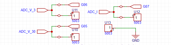
Figure 4-4 Sampling Circuit Connection Pins
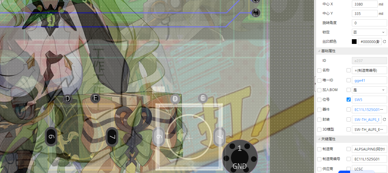
After arranging the pins, the hardware pins of the TFT screen are: G09-BL, G10-CS, G11-DC, G12-RES, G13-SDA, G14-SCL. The hardware pins of the rotary encoder are: G01-A1, G02-B1, G03-D1, G42-D2, G45-B2, G46-A2. The sampling section pins are: G06-ADC_V_3 (0~3V voltage sampling), G05-ADC_V_30 (0~30V voltage sampling), G07-ADC_I (current sampling).
4.2 TFT Screen Control
Here I'm using the Adafruit ST7735 library. In Arduino, you need to select "Library Manager," search for "Adafruit GFX Library," and install it. Then, similarly, search for "Adafruit ST7735 and ST7789 Library" in the Library Manager and install them. Below is the display after installation.

Figure 4-5: Adafruit ST7735 Library Installation Completed .
Using this library requires referencing "Adafruit_GFX.h" and "Adafruit_ST7735.h" beforehand. The code is as follows:
#include
#include
The following are the pin definitions. If you are using other pins to connect the TFT screen, you only need to modify these definitions. (The backlight pin, i.e., BL, can be set with a PWM for brightness control, or it can be left uncontrolled.)
#define TFT_CS 10
#define TFT_RST 12
#define TFT_DC 11
// Customize the SPI pin for ESP32
#define TFT_MOSI 13
#define TFT_SCLK 14
Some functions in this library are used as follows:
// Initialize the TFT object
Adafruit_ST7735 tft = Adafruit_ST7735(TFT_CS, TFT_DC, TFT_RST);
// Initialize the display
tft.initR(INITR_BLACKTAB);
// Fill the screen color
tft.fillScreen(ST7735_BLACK);
// Set the screen to landscape mode
tft.setRotation(3); // 0: default, 1: 90 degrees, 2: 180 degrees, 3: 270 degrees
// Set the text size
tft.setTextSize(2.5);
// Set text position
tft.setCursor(0, 0);
// Set text color
tft.setTextColor(ST77XX_BLUE); tft.setTextWrap(true);
// Display text content
tft.print("Voltmeter");
Drawing functions:
// Draw lines
// tft.drawLine(0, 0, 127, 159, ST7735_RED);
// // Draw rectangles
// tft.drawRect(10, 10, 50, 30, ST7735_GREEN);
// tft.fillRect(70, 10, 50, 30, ST7735_BLUE);
// // Draw circles
// tft.drawCircle(30, 90, 20, ST7735_YELLOW);
// tft.fillCircle(90, 90, 20, ST7735_CYAN);
// // Draw a triangle
// tft.drawTriangle(30, 130, 50, 160, 10, 160, ST7735_MAGENTA);
// tft.fillTriangle(90, 130, 110, 160, 70, 160, ST7735_ORANGE);
The usage of the TFT screen is essentially not much different from that of the serial port, so the above content is simple enough to control the TFT screen to achieve this project. In version 2 (v1.0) of
4.3 Encoder Control
, I used pins 1 and 2 for the encoder module, not noticing that these two pins are mainly used for UART0. Here, I intend to prevent the encoder from occupying UART0. Also, since only one rotary encoder is needed for interaction besides the oscilloscope, I only used the rotary encoder pins 45 and 46 in my program. The two buttons on the rotary encoder module are enabled, used as needed.
I used the Encoder library, which can easily process rotary encoder signals and calculate the direction and position of rotation. In the Arduino IDE, select the Library Manager (Sketch -> Include Library -> Manage Libraries). Search for "Encoder" and install Encoder by Paul Stoffregen.
In this library, we need to use its own `read` function to read the changed level each time the level changes, in order to determine the current state. Therefore, we use hardware interrupts to read the state.
The following are the configuration functions for the hardware interrupts on pins 45 and 46:
`attachInterrupt(digitalPinToInterrupt(46),handleEncoder2,CHANGE);//Encoder 2A phase` `
attachInterrupt(digitalPinToInterrupt(45),handleEncoder2,CHANGE);//Encoder 2B phase`
The following is the definition of the hardware interrupt function (`handleEncoder2`):
`void IRAM_ATTR handleEncoder2() {
// Interrupt service routine code
myEnc2.read();
}`
Here, `IRAM_ATTR` is a compiler instruction specific to ESP32 (and ESP8266) used to place functions or variables in the ESP32's internal RAM (IRAM). Its main function is to optimize the execution speed and response time of interrupt handling functions.
Note that the size of this RAM is limited; try to only put hardware interrupts in it, and also pay attention to the code size.
4.4 Analog-to-Digital Conversion (ADC)
For this section, I recommend referring directly to the official documentation. The documentation is comprehensive, and the functionality we're using isn't complex, so you can follow it directly. The address is: https://wiki.lckfb.com/zh-hans/esp32s3r8n8/arduino-beginner/adc.html
If you want to use a high sampling rate, it's recommended to switch to ESP-IDF and use DMA for development. This project uses timer interrupts for medium-speed (1-10k) sampling.
Before using timer interrupts, we need to test the execution time of the ADC read code (analogRead). Compile and burn the "ESP32_ADC_Time.ino" file in the appendix. We can calculate the average execution time by repeatedly executing this code 10,000 times to get the number of microseconds required for one execution of this code. The file also has comments; you can change the testing method according to your needs, such as executing this function multiple times, or executing other functions simultaneously.

Figure 4-6 shows the execution results of the “ESP32_ADC_Time.ino” file.
It indicates that executing 10,000 times took 301,485 microseconds, meaning each execution takes approximately 30 microseconds. A 10kHz sampling rate requires interrupt code execution time to be less than 100 microseconds, suggesting that a simple read operation can meet the 10kHz sampling rate requirement. However, further verification in actual measurements is needed, as interrupt propagation and other processes also require time.
However, when using the timer, the timer configuration function reported an error. After investigation, it was found to be an SDK version issue. Simply follow the tutorial to set the SDK version to the same version.
The previous version was 3.0.3; after uninstalling and changing the version number on the left to 2.0.14, the function compiled correctly. It's speculated that the library functions in the SDK were modified. Since Arduino development is chosen for its simplicity and speed, it's better to directly change the SDK version than to investigate the underlying issues.

Figure 4-7 shows the ESP32 SDK version .
In the actual project, two timers were used: one for sampling and the other for periodically triggering sampling. The following is the data obtained by sampling a 1kHz square wave with an input amplitude of 3.3V at 10kHz. One cycle contains 10 data points, proving that the frequency of the written timer interrupt function is correct (i.e., the function can complete within 100 microseconds).

Figure 4-8 shows the square wave test results.
Changing the value of "SAMPLE_SIZE" changes the sampling rate, and the size of the storage array also changes accordingly.
The corresponding program is stored in "ESP32ADC_TEST.ino", which you can download and test yourself.
4.5 Overall Program
Due to time constraints, and because this is my first time writing ESP32 Arduino code, oscilloscope mode and spectrum analyzer mode were difficult to complete within the time limit. Therefore, I first wrote a simple display interface.
Later, I will update the oscilloscope and spectrum analyzer modes, adjusting them through the encoder, and also change the encoder pins to make the right encoder usable. (The underlying implementation is already possible; the main challenge is writing the interface. If you are interested in this project, please help me write it!)
The program is stored in "VoltmeterAndAmmeter.ino". See the demonstration video for a tutorial.
The top layer of the 3D shell is relatively thin; it is recommended to thicken it, otherwise the printing effect will be poor. The layer thickness has little impact after adding the panel. (Just like phone case back covers, some are poorly made and some are well-made, but once you put a phone case on, they all look the same.)
The panel is under improvement; you can add other panels in the file to avoid waste.
Finally, I am very grateful to the teacher for the detailed documentation and comprehensive video explanations. I learned a lot.
Documentation address:
https://wiki.lckfb.com/zh-hans/dwx-cw32f030c8t6/training/voltammeter-bootcamp/voltammeter.html
Video address: https://www.bilibili.com/video/BV1Hw4m1k7PK/
Also, refer to
the official ESP document:
https://www.espressif.com/sites/default/files/documentation/esp32-s3_datasheet_cn.pdf (chip manual)
[https://docs.espressif.com/projects/esp-hardware-design-guidelines/zh_CN/latest/esp32s3/schematic-checklist.html#adc](Hardware Design)
[https://www.espressif.com/sites/default/files/documentation/esp32-s3_technical_reference_manual_cn.pdf#resclk](Technical Documentation)
[MPY Software Development:
http://t.csdnimg.cn/npC93](Screen Driver)
[ADC Section:
http://t.csdnimg.cn/OaQyu](Understanding LSB (Bit LSB, Analog-to-Digital Conversion LSB)) [
Current Sampling Section:
http://t.csdnimg.cn/uZ7rP](Current Sensing Amplifier Guide - TI High Precision Lab)
[http://t.csdnimg.cn/ckecA](Op-amp - Resistive Current Sampling - High-Side and Low-Side Current Sampling Schemes))
https://www.ti.com/cn/lit/ds/symlink/ina199.pdf?ts=1722388537150&ref_url=https%253A%252F%252Fclient%252F (INA199 chip manual)
https://oshwhub.com/limengmeng12345/ji-chu-ying-usb-dian-ya-biao (open source project)
Design a simple oscilloscope based on CW32, displaying waveforms on a 1.8-inch TFT screen; supports waveform scaling and pause display; supports PWM output of 1K, 2K, and 4K square wave signals with adjustable duty cycle. Supports frequency measurement below 100KHz.
Function Description:
1. Data Acquisition: Single-channel data acquisition using the core board's ADC function.
2. Adjustable Signal Attenuation: Through resistor voltage division, it can be set to 50X, 10X, etc., with 10X recommended.
3. Supports PWM square wave output: 1K, 2K, 4KHz output, with adjustable duty cycle in 5% steps.
4. Waveform Display: Displayed on a 1.8-inch TFT screen with a resolution of 128X160.
5. Compatible with multiple core boards including CW32, GD32, and STM32.
6. Supports Frequency Measurement: Achieved through the MCU's GPIO capture function.
7. Reserved sensor interfaces, such as temperature and humidity sensors, barometers, etc.
Design Background
: Oscilloscopes are indispensable tools for electronic engineers. They are divided into analog and digital oscilloscopes based on the signal type. Analog oscilloscopes use analog circuits and electron guns to display waveforms by projecting an electron beam onto the screen, while digital oscilloscopes use digital circuits and digital storage technology to digitize and display the waveform.

Analog Oscilloscopes vs. Digital Oscilloscopes (e.g., Rigol DS6104):
In the process of oscilloscope upgrades and iterations, traditional analog oscilloscopes can no longer meet the needs of modern electronic measurements. Compared to analog oscilloscopes, digital oscilloscopes offer higher measurement accuracy, more stable display, and better signal transmission. With technological advancements, the performance and functionality of oscilloscopes continue to improve. Modern oscilloscopes utilize technologies such as high-speed ADCs and FPGAs, featuring high bandwidth, high sampling rates, and deep memory depth. Furthermore, digital oscilloscopes support various triggering methods and signal analysis functions, such as FFT transformation and spectrum analysis.
To learn how to use the CW32 core board as the main controller, this study will explore the construction method of a simple oscilloscope.
The implementation process involves
circuit principle analysis
. A digital oscilloscope is an instrument used to display electrical signal waveforms, mainly composed of analog front-end processing circuits, microcontroller circuits, power supply circuits, control circuits, triggering circuits, calibration circuits, and other circuits. As this project is an introductory oscilloscope project, several core circuits were selected in the circuit design to help beginners better understand the principles and design methods of oscilloscopes. These mainly include the following circuits:
Analog front-end processing circuit: responsible for processing the input analog signal and then sending it to the microcontroller for identification. Specific circuits include AC/DC coupling selection circuit, voltage attenuation circuit, signal processing circuit, and frequency detection circuit, which is the core of the entire circuit.
Power supply circuit: responsible for providing positive and negative power to the operational amplifier and system power, ensuring the normal operation of the circuit.
Microcontroller circuit: provides the control core of the system, responsible for the acquisition, processing, and output of input signals.
Human-machine interface circuit: used to control oscilloscope functions, including buttons, knobs, LEDs, display screen, and other input/output interfaces, providing a foundation for the development of oscilloscope functions.
Schematic Design of
Analog Front-End Processing Circuit
: In the entire oscilloscope circuit design process, the analog front-end processing circuit is the most important. It extensively utilizes knowledge of analog circuits, including an input AC/DC coupling switching circuit, an input signal attenuation circuit, and a signal conditioning circuit.

The AC/DC coupling switching circuit
can classify signal types into DC and AC signals. Real-world signals are often not ideal waveforms. For example, a DC power supply signal should be a horizontal DC signal, but it will always contain power supply ripple (AC signal). When acquiring AC signals, DC signals may also be mixed in, affecting the peak-to-peak value of the waveform. To ensure accurate measurement of the input AC signal, the characteristic of a capacitor to pass AC and block DC is utilized. By connecting a capacitor in series with the circuit, the DC component in the signal can be filtered out; this is the concept of AC coupling. DC coupling, on the other hand, involves not processing the input signal in any way.

The input signal attenuation circuit,
after passing through the AC/DC coupling selection circuit, uses switch SW3 to select two channels. When switches 2 and 3 are connected together, the input signal flows directly into the subsequent voltage follower circuit. When switches 2 and 1 are connected together, the input signal is attenuated to 1/50th of its original value after passing through a resistor divider network composed of resistors R8, R12, and R15. That is,
when switches 2 and 1 are connected together, the measurable input signal amplitude is -1.6V to 5V;
when switches 2 and 3 are connected together, the measurable input signal amplitude is -80V to 250V.
Therefore, when the input signal amplitude is small, the lower voltage range should be selected first. If the input signal amplitude is uncertain during measurement, the higher voltage range can be used first. If it falls within the lower voltage range, the lower voltage range can be used to obtain a more accurate measurement result, while simultaneously protecting the circuit.

The signal conditioning
circuit includes a voltage follower and a signal amplification circuit composed of operational amplifiers. When analyzing this part of the circuit, it is necessary to understand the virtual open and virtual short principles of operational amplifiers.

(1) Voltage Follower Circuit:
In the U6.2 chip, the inverting input pin 2 of the op-amp is connected to the output pin 1 of the op-amp. Combined with the virtual short characteristic of the op-amp, V+=V-=Vout. According to the virtual open circuit, the input impedance of the op-amp is relatively large, so the forward input current of the op-amp is very small. The output impedance of the op-amp is small, so the output current is very large. It is said that the voltage follower here plays the role of impedance matching.
(2) Proportional Amplifier Circuit
: When analyzing the circuit composed of the op-amp U6.1, it can be decomposed into a non-inverting proportional amplifier circuit and an inverting proportional amplifier circuit for separate analysis and then combined together.
Low voltage range measurement range: -1.6V~5V, high voltage range measurement range: -80V~250V.
Comparator Frequency Measurement Circuit :
In order to realize the frequency detection function, the ADC input signal is compared with the input signal through a hysteresis comparator to realize the frequency measurement function. A hysteresis comparator is a type of voltage comparator. A conventional voltage comparator is a single-threshold comparator, meaning the circuit has only one threshold voltage. However, even a small change in the input voltage near the threshold will cause a significant change in the output voltage. To enhance the circuit's anti-interference capability, positive feedback is introduced into the single-threshold comparator, ensuring signal stability within a certain range. The hysteresis comparator circuit outputs a square wave signal, and the microcontroller's timer capture function is used to calculate the period of the input waveform.

The rotary encoder circuit
is a special type of button. The EC11 rotary encoder used in this project has five pins. Pins D and E are similar to ordinary button pins; they are activated when pressed and deactivated when released. The remaining three pins,
A, B, and C, are used to detect the rotation direction of the knob. Pin C is the common terminal and can be directly grounded. During rotary encoder operation, there is a phase difference between the A and B signal pins. That is, a change in the signal on one pin precedes a change in the signal on the other pin; the two pins do not change simultaneously. By detecting which pin changes first, the clockwise or counterclockwise rotation function can be determined.

The LED indicator circuit
is relatively simple in design, using a low-level drive method. When the microcontroller pin outputs a low level, a potential difference exists across the LED, and the LED lights up; when the microcontroller pin outputs a high level, the LED turns off.

Key input detection circuit.
In addition to the rotary encoder, this project also uses four independent buttons to control the system. One side of each button is directly grounded, and the other side is connected to a microcontroller pin. When the microcontroller pin detects a button press, it connects directly to GND (Ground). The microcontroller receives this grounding signal and then executes the corresponding function. To save hardware costs, debouncing can be introduced in the software design to avoid false triggering due to mechanical button bounce.

The main controller selected
is the LCSC CW32F030C8T6 development board, a microcontroller development board based on the ARM Cortex-M0 core, provided by LCSC Mall (LCSC website). The following is a detailed introduction to this development board:
Basic Information
: Brand and Model: LCSC development board, model LCKFB-DWX-CW32F030C8T6.
Processor: Equipped with a CW32F030C8T6 microcontroller, a 32-bit MCU based on the ARM Cortex-M0 core, suitable for low-power, high-performance embedded applications.
Features and Functionality
Extensibility: Offers rich expansion interfaces, such as the SMT extension library, facilitating secondary development and functional expansion according to user needs.
Debugging and Programming: Supports efficient debugging and program burning using debugging tools such as J-Link, improving development efficiency. It also supports programming in development environments such as Keil.
Low Power Consumption: Utilizing a Cortex-M0 core, this development board features low power consumption, suitable for applications with strict power requirements.
Accessories and Documentation
: Accessories: Typically, this development board comes with two 1x20P straight headers, one 1x4P right-angle header, and one instruction manual. Please note that these accessories may not be covered by after-sales service. Documentation:
A detailed datasheet (PDF format) is provided, which users can download and consult through channels such as LCSC Online Store for better understanding and use of the development board.
Purchase and Inventory
Pricing: According to LCSC Online Store, the price of this development board is relatively affordable; however, the specific price may vary due to promotional activities and other factors.
Inventory: LCSC Online Store has warehouses in Jiangsu and Guangdong, with ample inventory, so users can purchase with confidence.
Development and Usage
: It is recommended to use an Integrated Development Environment (IDE) such as Keil for program development. These environments provide rich features and tools, helping users get started quickly and develop efficiently.
Application Scenarios: Due to its low power consumption and high performance, the LCSC Diwenxing CW32F030C8T6 development board is suitable for various embedded application scenarios, such as smart homes, industrial automation, and IoT devices.
In summary, the LCSC Diwenxing CW32F030C8T6 development board is a cost-effective and feature-rich microcontroller development board suitable for a wide range of embedded developers. The 1.8-inch TFT

LCD display circuit
is a color display with 128 x 160 color pixels. It connects to the microcontroller using a four-wire SPI communication method, with a total of eight pins. The module pin description and connection to the microcontroller are as follows:
Pin Number
Pin Name
Pin Description

1. GND Power Ground Pin
2 VCC Power Supply 3 SCL SPI Serial Clock Signal 4 SDA SPI Data Pin (MOSI) 5 RES Reset Pin 6 DC Command and Data Select Pin 7 CS LCD Chip Select Pin 8 BL Backlight Pin The power supply design supports lithium battery power and USB power. USB charging is used. Other circuits, in addition to the oscilloscope detection function, have a separate PWM signal to simulate a simple function generator function. By changing the frequency and duty cycle of the output PWM, a simple square wave signal can be output. A sensor interface is also reserved, supporting AHT21 and BMP280 access. The PCB design is carried out using LCEDA open source software. The layout design is compact, convenient and practical. The trace design should be as short as possible. Based on EMC and EMI principles, wire diameter and vias should be designed, and power traces should be designed according to load capacity and current carrying capacity. Ground segmentation is implemented to separate analog and digital grounds. The enclosure design uses LCEDA open-source software, paying particular attention to precise hole placement and tolerance allowances; otherwise, installation will be impossible. The panel design also uses LCEDA open-source software, again emphasizing the importance of precise hole placement and tolerance allowances; otherwise, misalignment will be unsightly and installation will be difficult. Labels should be clear, accurate, and easily identifiable. The main control code implementation of the program is as follows: #include "main.h" #include "tft.h" #include "tft_init.h" #include "led.h" #include "adc.h" #include "timer.h" #include "freq.h" #include "key.h" void RCC_Configuration(void); volatile struct Oscilloscope oscilloscope={0}; void Init_Oscilloscope(volatile struct Oscilloscope *value); extern uint16_t adc_value[ADC_VALUE_NUM]; int main() { uint16_t i=0; // intermediate value float median=0; // peak-to-peak value


float voltage=0,vpp=0;
// Trigger voltage value
float max_data=2.5f;
// Waveform amplification factor
float gainFactor=15.0f;
// Trigger edge marker
uint16_t Trigger_number=0;
// Initialize oscilloscope parameters
Init_Oscilloscope(&oscilloscope);
// Clock initialization
RCC_Configuration();
// LED initialization
Init_LED_GPIO();
// Screen initialization
TFT_Init();
// Initialize ADC pins
Init_ADC(oscilloscope.ADC_ClkDiv,oscilloscope.ADC_SampleTime);
// ADC DMA initialization
ADC_DMA_Init();
// Fill with black
TFT_Fill(0,0,160,128,BLACK);
// Initialize PWM output
Init_PWM_Output(oscilloscope.timerPeriod-1,oscilloscope.pwmOut);
// Initialize EC11 pin
Init_EC11_GPIO();
// Initialize button pin
Init_Key_GPIO();
// Initialize frequency timer
Init_FreqTimer();
// Initialize static UI
TFT_StaticUI();
while(1)
{
// Key scan processing function
Key_Handle(&oscilloscope);
if(oscilloscope.showbit==1)
{
oscilloscope.showbit=0;
oscilloscope.vpp=0;
// Convert voltage value
for(i=0;i
{
oscilloscope.voltageValue[i]=(adc_value[i]*3.3f)/4096.0f;
// Get peak voltage of the entire data segment
vpp=(5-(2.0f*oscilloscope.voltageValue[i]));
if((oscilloscope.vpp)
{
oscilloscope.vpp = vpp;
}
if(oscilloscope.vpp
{
oscilloscope.gatherFreq=0;
}
}
// Find the starting display waveform value
for(i=0;i
{
if(oscilloscope.voltageValue[i]
{
for(;i
{
if(oscilloscope.voltageValue[i] > max_data)
{
Trigger_number=i;
break;
}
}
break;
}
}
// If the amplitude is too small, the amplification factor will be too large, causing the waveform display to be abnormal.
if(oscilloscope.vpp > 0.3)
{
// Calculate the intermediate amplitude. The lowest input point is 2.5V, and the highest is (5-vpp)/2. T
 Software Code
  Pressing button 1 for the first time switches to fan speed adjustment; the default is 0, and the fan will rotate as long as it is not 0.
  Pressing button 2 switches to time adjustment; heating begins when the time is not 0. Pressing button 2 switches to seconds, minutes, and hours, adjusted by the rotary encoder. Pressing
  button 1 a third time switches to automatic mode, sets the temperature to 39 degrees Celsius, and uses the rotary encoder to adjust the on/off state. The idea is to automatically stop based on humidity data, but the humidity data fluctuates significantly, requiring further testing to confirm its feasibility (code not yet written). Currently, the temperature is set to 39 degrees Celsius, the fan is at 90% capacity, and it runs continuously.
  Pressing button a fourth time returns to the first state.
  shows a box of newborn puppies.
 1.1 Power Supply Chip Selection
  Figure 1-1 shows the schematic diagram of the LCKFB-ESP32S3 power supply circuit
  Figure 1-2 DC-DC Circuit Design Reference
  Figure 1-3 shows an example project in the electrical section of the ADC chip manual,
  Figure 1-4 INA199 Chip Manual
  Figure 2-1 DC 9-12V Power Input Circuit
  Figure 2-2 Voltage Sampling Circuit)
  Figure 2-3 Hardware Design Guide Recommendation
  Figure 2-4 Typical Application of INA199
  Figure 2-5 Current Sampling Circuit
  Figure 2-6 Test Point and Pin Connection
  Figure 2-8 Test Point Package Attributes
 At the same time, some space is reserved to prepare for adding other functions later.
  Also, in the second version, I placed the power supply section on the left side, with separate copper plating, to provide some isolation.
  Figure 3-1: Component shape in PCB design
  Figure 4-4 Sampling Circuit Connection Pins


 京公网安备 11010802033920号

 1KS068-50TG


