The NE555+CD4017 electronic turntable with sequential lighting can be used for decision-making. This was a case study from the first training session for lecturers at Northwest University.
A toggle switch is used for switching between sequential lighting modes, and a tactile switch is used for decision-making mode.
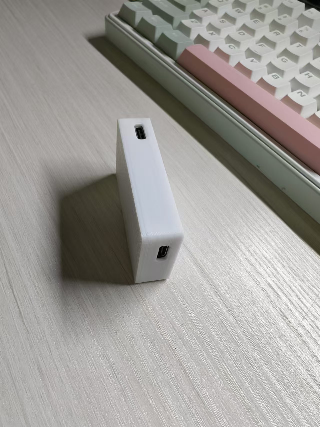
A base plate the same size as the Orange Pie CM4, measuring only 55*40 mm.
The voltage and current meter is based on CW32 and is compatible with STM32F103C8T6 in design.
Compared to the official project: 1. A CH340N serial port has been added, enabling communication with the microcontroller via USB for convenient data acquisition; 2. A WS2812 LED has been added, allowing for more visually appealing designs;
3. Six NPN transistors are used to drive the digital tube, reducing the microcontroller's current consumption;
4. ESD protection has been added to the interface to enhance electrostatic discharge protection;
5. The digital tube adopts a common anode design.
Functions: Main control chip: STC32F; DI: 4-channel optocoupler input; DO: 4-channel transistor output; Network: 3-channel RS485; Power supply: 24V;
Functions: Main control chip: STC32F; DI: 8-channel optocoupler input; DO: 4-channel transistor output; Network: 3-channel RS485; Power supply: 24V;
Using a CW chip, and employing ADC and SPI, current and voltage display outputs are achieved.
Project Introduction
This project is a current and voltage meter based on the CW32 microcontroller.
Project Functions
This design is a current and voltage meter based on the CW32 microcontroller for detection; it uses a 0.96-inch OLED screen to display the detected current and voltage; it uses a voltage divider circuit to expand the detected voltage and current range; it has a button to switch modes; and it uses LED technology to indicate the status.
Project Parameters
This design uses the CW32 main control chip with an internal reference, ensuring accurate ADC acquisition;
it uses a 0.96-inch OLED display to refresh the displayed current and voltage in real time;
it uses a voltage divider circuit to expand the measurement range;
Principle Analysis (Hardware Description)
This project consists of the following parts: power supply section, LED indicator, main control section, ADC acquisition, and OLED display section. This project mainly acquires data through the ADC, processes it, and displays it on the OLED screen.
1--Main Control Circuit:
Uses a CW32 chip with a serial port for easy debugging.

2--Power Supply Circuit:
Uses a TYPE-C-16P interface as the power supply interface, with reverse connection protection.

3--OLED Display Circuit:
Uses a 0.96-inch OLED display screen; there are many tutorials available, making display porting convenient.

4--The ADC acquisition circuit
uses a voltage divider circuit to expand the range.

5--The reference circuit
provides a reference, making the measurement more accurate.

6--The calibration circuit
is used because the measurement circuit has errors; calibration can be performed later.

Software code
1--Uses the RT-Thread operating system, a very small kernel version, and is integrated with finsh.
void rt_hw_console_output(const char *str)
{
rt_size_t i = 0, size = 0;
size= rt_strlen(str);
for(i=0 ; i < size ;i++)
{
if (*str == '
')
{
USART_ClearFlag(CW_UART1, USART_FLAG_TC);
USART_SendData_8bit(CW_UART1, '
');
while(USART_GetFlagStatus(CW_UART1, USART_FLAG_TC)== RESET);
}
USART_ClearFlag(CW_UART1, USART_FLAG_TC);
USART_SendData_8bit(CW_UART1, *(str++));
while(USART_GetFlagStatus(CW_UART1, USART_FLAG_TC)== RESET);
}
}
int rt_hw_console_getchar(void)
{
int ch = -1;
while (USART_GetFlagStatus(CW_UART1, USART_FLAG_RC) == RESET);
USART_ClearFlag(CW_UART1, USART_FLAG_RC);
if (USART_GetFlagStatus(CW_UART1, USART_FLAG_PE | USART_FLAG_FE))
{
USART_ClearFlag(CW_UART1, USART_FLAG_PE | USART_FLAG_FE);
rt_thread_mdelay(10);
}
else
{
ch= USART_ReceiveData_8bit(CW_UART1);
}
return ch;
}
2--OLED displays
use hardware SPI and also port U8G2. For OLED porting, please refer to the LCSC porting manual.
uint8_t u8x8_byte_4wire_hw_spi(u8x8_t *u8x8, uint8_t msg, uint8_t arg_int,
void *arg_ptr)
{
uint8_t *data = (uint8_t *)arg_ptr;
switch (msg)
{
case U8X8_MSG_BYTE_SEND:
{
for(int i = 0; i < arg_int; i++)
spi_read_write_byte((u8)*(data + i));
break;
}
case U8X8_MSG_BYTE_INIT:
break;
case U8X8_MSG_BYTE_SET_DC:
if ( arg_int ) GPIO_WritePin(OLED_GPIO_PORT,OLED_DC_PIN, GPIO_Pin_SET);
else GPIO_WritePin(OLED_GPIO_PORT,OLED_DC_PIN, GPIO_Pin_RESET);
break;
case U8X8_MSG_BYTE_START_TRANSFER:
GPIO_WritePin(OLED_GPIO_PORT,OLED_CS_PIN, GPIO_Pin_RESET);
break;
case U8X8_MSG_BYTE_END_TRANSFER:
GPIO_WritePin(OLED_GPIO_PORT,OLED_CS_PIN, GPIO_Pin_SET);
break;
default:
return 0;
}
return 1;
}
3--ADC Acquisition
After ADC acquisition, the output is filtered.
void ADC_init(void)
{
ADC_InitTypeDef ADC_InitStructure; // ADC configuration structure
ADC_SerialChTypeDef ADC_SerialChStructure; // ADC serial channel structure
GPIO_InitTypeDef GPIO_Init_Struct;
__RCC_GPIOB_CLK_ENABLE(); // Enable ADC clock for corresponding pin
__RCC_ADC_CLK_ENABLE(); // Enable ADC clock
PB00_ANALOG_ENABLE(); // Enable analog pin
PB01_ANALOG_ENABLE(); // Enable analog pin
PB10_ANALOG_ENABLE();
// Enable analog pin PB11_ANALOG_ENABLE(); // Enable analog pin
ADC_StructInit(&ADC_InitStructure); // Initialize ADC default values
ADC_InitStructure.ADC_ClkDiv = ADC_Clk_Div128; // Configure ADC operating clock PCLK/4 = 6/4 = 1.5MHz
// ADC_SerialChStructure.ADC_InitStruct.ADC_AccEn = ADC_AccDisable; // Disable accumulation of conversion results
// ADC_SerialChStructure.ADC_InitStruct.ADC_Align = ADC_AlignLeft; // Right-align ADC conversion results
// ADC_SerialChStructure.ADC_InitStruct.ADC_DMAEn = ADC_DmaDisable; // Disable DMA transfer
// ADC_SerialChStructure.ADC_InitStruct.ADC_SampleTime = ADC_SampTime5Clk; // 5 ADC clock cycles
// ADC_SerialChStructure.ADC_InitStruct.ADC_InBufEn = ADC_BufEnable; // Enable follower
// ADC_SerialChStructure.ADC_InitStruct.ADC_TsEn = ADC_TsEnable; // Disable built-in temperature sensor
// ADC_SerialChStructure.ADC_InitStruct.ADC_OpMode = ADC_SerialChScanMode; // Sequence scan mode: all 4 channels are converted simultaneously.
/* When the signal voltage is low, the reference voltage can be reduced to improve resolution. After changing the reference voltage, the same binary representation of the voltage value will be different.
The largest binary value (all 1s) represents your reference voltage, which needs to be taken into account when calculating the actual voltage. */ /*
ADC_InitStructure.ADC_VrefSel = ADC_Vref_BGR1p5; // Reference voltage set to 1.5V
ADC_InitStructure.ADC_SampleTime = ADC_SampTime10Clk; // Since the voltage signal is a slow signal, the ADC sampling time is ten ADC sampling cycles to ensure accuracy
ADC_SerialChStructure.ADC_Sqr0Chmux = ADC_SqrCh8; // Channel 4 input PB00
ADC_SerialChStructure.ADC_Sqr1Chmux = ADC_SqrCh9; // Channel 13 input
ADC_SerialChStructure.ADC_Sqr2Chmux = ADC_SqrCh11; // Channel 11 input
ADC_SerialChStructure.ADC_Sqr3Chmux = ADC_SqrCh12; // Channel 12 input
ADC_SerialChStructure.ADC_SqrEns = ADC_SqrEns03; //Sqr is the sequence configuration register. Since only the channel for sequence 0 is used here, configuring it to 0 indicates that only the Sqr0 sequence is being converted.
ADC_SerialChStructure.ADC_InitStruct = ADC_InitStructure; //ADC initialization
ADC_SerialChContinuousModeCfg(&ADC_SerialChStructure); //ADC sequence continuous conversion mode configuration
ADC_ClrAccResult();
ADC_ClearITPendingAll(); // Clear all ADC interrupt states
ADC_Enable(); // Enable ADC
ADC_SoftwareStartConvCmd(ENABLE); // Start ADC conversion software command
}
uint32_t Mean_Value_Filter(uint16_t *value, uint32_t size) // Mean filter
{
uint32_t sum = 0;
uint16_t max = 0;
uint16_t min = 0xffff;
int i;
for(i = 0; i < size; i++) // Iterate through the array to find the maximum and minimum values
{
sum += value[i];
if(value[i] > max)
{
max = value[i];
}
if(value[i] < min)
{
min = value[i];
}
}
sum -= max + min; // Subtract the maximum and minimum values and then calculate the average
sum = sum / (size - 2);
return sum;
}
4--Saving the calibration
After calibration, the corresponding values are latched in flash to prevent the values from changing after power-on. Here, the K values of voltage and current are calculated using a function. When writing, be sure to erase first and then write, otherwise a write error will occur.
`void flash_erase(void)
{
uint8_t Flag;
// erase
FLASH_UnlockPages(START_ADDR, END_ADDR);
// Unlock the last page Flag = FLASH_ErasePages(START_ADDR, END_ADDR); // Erase the last page
FLASH_LockAllPages();
}
void flash_write(uint16_t offset,uint16_t *data,uint16_t lenght)
{
uint8_t Flag;
// write
FLASH_UnlockPages(START_ADDR, END_ADDR); // Unlock the last page
Flag = FLASH_WirteHalfWords(START_ADDR+offset*2, data, lenght);
FLASH_LockAllPages();
}
void ComputeKV()
{
flash_read(0,k_data,4);
flash_erase();`
k_data[0]=cal_adc.span_v[1]-cal_adc.span_v[0];
k_data[0]= (k_data[0]/(V_15-V_05));//Voltage
k_data[2] = 8;
flash_write(0,k_data,4);
}
void ComputeKI()
{
flash_read(0,k_data,4);
flash_erase();
k_data[1]=cal_adc.span_m[1]-cal_adc.span_m[0];
k_data[1]= (k_data[1]/(M_15-M_05));//Current
k_data[3]=8;
flash_write(0,k_data,4);
}
Function Description
1. The current measurement range displayed on the main interface is 0~3A, the voltage range is 0~3V, and the VMAX range is 0~30V, which is one-to-one with the measurement range of the hardware circuit;
2. Button instructions:
(1) K1 Main interface switch;
(2) K2 Click the interface to display calibration mode and enter calibration;
(3) K3 Current/voltage calibration, click to switch;
(4) K4 Click for the first time to enter the first calibration point, click again to record the calibration value and end;
(5) K4 Click for the first time to enter the second calibration point, click again to record the calibration value and end;
(6) After calibrating two points, click K6 to calculate the K value and end the calibration;
(7) Each button corresponds to an indicator light.
Physical demonstration
: 5V voltage is measured, 3V circuit displays 3V, full scale, 30V range displays an error of 5.1V.

Subsequent optimization
: OLED design is designed as a multi-level interface;
use buttons to switch (6 buttons are reserved, no hardware changes are required);
Attachment list:
1. CWF030 is the source code;
2. C5138758 is the OED screen specification sheet, which contains the driver process;
3. PCtoLCD2002 is a commonly used mold extraction software.
A small board that automatically downloads firmware for ESP series chips, saving development board size and components.
The STM32IGT6 development board, designed based on the Zhengdian Atomic development board, has been functionally verified and works without issues. It includes an onboard serial port module.


 Images of images
  are
are  included.
  ]
]  Update 9.15: New version verified
  .]
.]  ![IMG_20240910_163859.jpg]
  9.25 Update: Power supply changed to 6-pin Type-C
 camera, and
  display


 You can use the official flash tool, or the Platform.io plugin in VS Code, or the espidf plugin in VS Code. Self-testing shows successful downloads, so you can use them with confidence.


 京公网安备 11010802033920号

 NRLM332M350V22X30F


