1. Input/
output interfaces: Type-C and XT30 interfaces are used.
2. Power supply
: LDO (SE8550K2) is used to regulate the power supply to 5V, supporting a maximum input of 35V.
3. Voltage measurement:
Resistor voltage divider is used, followed by ADC sampling.
4. Current measurement
: INA199 amplifies the voltage across the sampling resistor and supports bidirectional current.
5. PD spoofing:
. 6. Display:
0.96-inch OELID screen displays voltage, current, power, etc.
7. Actual product image .
Design and fabrication of a voltage and current meter using the JLCPCB CW32 development board.
1. Function Introduction
This project uses the JLCPCB CW32 development board to design and fabricate a voltage and current meter. Currently, it can
measure voltage, current, capacitance, and resistance with high accuracy.
2. Schematic Diagram Description
2.1 Power Supply Circuit
Considering the portability and ease of use of the voltage and current meter, a USB + lithium battery power supply scheme is adopted. When the USB socket is plugged in, the system is powered by the USB and charges the lithium battery; when the socket is unplugged, the entire power supply is provided by a single 18650 lithium battery.

2.2 Automatic Switching of Power Supply Circuit
The key to achieving automatic switching of the power supply circuit lies in the use of a PNP MOSFET. When the MOSFET's voltage is Vgs0, it is cut off, and the lithium battery does not supply power. When only the lithium battery is supplying power, point G is grounded, and the voltage is 0V.
2.3 5V Boost Circuit
Although lithium battery power is convenient, the battery voltage cannot reach 5V, and it will further decrease with use. Therefore, a boost chip is needed to boost the voltage to 5V. The boost converter chip used in this project is the X4310 from Chipstar. This chip has a fixed output of 5V when the input is 2.7~5V, and it also has current limiting protection—when the output current exceeds 300mA, the chip will limit the current to 300mA, ensuring the safety of the entire system.

2.4 Lithium Battery Charging and Discharging Management Circuit
Regarding the lithium battery charging and discharging circuit, the commonly used TP4054 charging and discharging management chip was used. It has a maximum charging current of 500mA, which can be adjusted by changing the resistor. During charging, pin 1 of the chip is grounded, and the LED lights up. When the battery is fully charged, pin 1 switches to a high state, and the LED turns off. The battery charging status can be determined by the LED's on/off state.

2.5 Display Circuit:
The display circuit uses a 0.96-inch OLED screen. This screen communicates via I2C, requiring only 4 pins to achieve real-time data display, significantly reducing I/O resource usage.

2.6 Key Control Circuit:
Key recognition in this project uses an interrupt-driven approach. A 100nF capacitor is added around each key for filtering and debouncing. Verification has shown that this method provides high accuracy in key detection, preventing issues like unresponsive keys or double-clicks when a single key is pressed.

2.7 Current and Voltage Sampling Circuit:
The voltage sampling circuit uses a 1% accuracy voltage divider resistor to divide the voltage before it enters the MCU's ADC acquisition port. Diodes D3 and D5 limit the voltage here, preventing high voltage from entering the acquisition port and damaging the MCU. During voltage sampling, the voltage is first attenuated by 21 times before being acquired by the MCU's ADC pin and compared with an internal reference voltage. The output voltage value is then determined (if the output is less than 3V, a 2x attenuation channel is switched for re-conversion to improve measurement accuracy). The internal reference voltage is selected as 1.5V; the current sampling is similar, except that the resistor in the voltage attenuation circuit is replaced with a 100mΩ sampling resistor, and the circuit current is obtained by reading the voltage of the sampling resistor using an ADC.

2.8 Resistance and Capacitance Measurement
This resistance and capacitance measurement utilizes the principle of NE555 square wave generation. First, the capacitor and resistor to be measured are connected to the NE555 circuit, causing the NE555 circuit to output PWM waves of different frequencies. Then, the PWM waveform frequency is captured using the CW32 input capture function. Finally, the values of the resistor and capacitor to be measured are calculated. The specific calculation steps are as follows:

The above figure shows the wiring diagram when the NE555 generates a square wave. The formula for calculating the frequency and duty cycle of the square wave is as follows (period: T, frequency F, duty cycle: D):

Therefore, to measure capacitor C1, it is only necessary to control R1 and R2 to constant values and calculate according to the PWM frequency F captured by the MUC. The formula is: C1=1.44/(R1+2*R2)*F).
Similarly, the value of resistor R2 can be calculated using the formula: R2=1.44/(2*F*C1)-R1/2.

3. Physical Diagram

4. PCB Design Notes
In the PCB design, the power supply traces should be thickened, and copper pours should be used for connection when necessary.

When designing the current testing circuit, considering that the path will pass through a maximum current of 3A, it is essential to use full-connection copper plating on the pads, and the copper width must be wide to prevent the PCB from overheating due to high current, which would affect measurement accuracy.

5. Key Program Descriptions
5.1 Button Recognition Interrupt Configuration

When initializing the IO port, it is necessary to configure the external interrupt trigger condition and then enable the external interrupt.
Interrupt Service Function:

In this project, all GPIO ports share one interrupt service function. The function determines which IO port to interrupt and updates the flag bit.
5.2 ADC Configuration

In ADC conversion, three ADC ports are required. Therefore, multi-channel conversion is necessary when configuring the ADC, and it is important to ensure that the corresponding ADC conversion channel is enabled.
5.3 Timer Configuration
Timers were used for both resistor and capacitor tests. The timer configuration is as follows:

Initially, one timer with two channels was used to complete the input capture, but it was found that the same timer input capture interrupt start flag only had one bit, which could not capture two PWM waves of different frequencies simultaneously.
Ultimately, two timers were used.
6. Material Purchase
In this project example, all materials can be purchased from LCSC Mall. LCSC Mall is recommended!
7. Assembly Instructions:
All resistors and capacitors in this project use 0603 packages. Beginners can easily replace them with plug-in packages to reduce soldering difficulty. The casing and PCB are fixed with 4 M3 screws. The 18650 lithium battery is placed inside the casing.
Experience the functions and performance of the Diwenxing CW32 development board and design a voltage and current meter.

I. Design Background
I was pleased to learn about and become familiar with a domestically developed development board during the summer: the LCSC CW32F030C8T6 development board. My learning and practical focus was on a voltmeter and ammeter.

Digital voltmeters and ammeters combine ADC technology with circuit measurement principles, accurately converting analog voltage and current signals into digital displays for easy reading and analysis by electronic engineers. This device not only improves the accuracy and efficiency of circuit measurements but also helps engineers better understand circuit behavior, making it a powerful tool for electronic design and troubleshooting, and playing a crucial supporting role in the work of electronic engineers. In product applications, digital voltmeters ensure the accuracy and safety of circuit design, while also providing strong support for product quality control and subsequent maintenance.
An ADC (Analog-to-Digital Converter)
is an indispensable key component in electronic systems, converting continuous analog signals into digital signals, enabling digital processing and analysis. ADCs play a crucial role in signal conversion, measurement and data acquisition, control system input, and communication and signal processing. Their widespread application promotes the intelligent and precise control of electronic equipment in various industries and is one of the key factors driving modern technological progress.
II. Design Approach
Learning to design and build a digital voltmeter and ammeter is highly beneficial for improving personal professional skills. The digital voltmeter and ammeter project covers multiple aspects, including microcontroller circuit design and implementation, signal acquisition and processing circuit design, user interface development and optimization, and product appearance design. It integrates knowledge from multiple fields such as electronic technology, microcontroller programming, circuit design, and industrial design. This project has the following highlights:
It adopts a core board plus expansion board design concept and uses plug-in device design, making learning simpler and exploration more in-depth;
the core board uses the domestic Wuhan Xinyuan Semiconductor CW32 as the main controller, while also being compatible with other similar development boards; however, the CW32 has advantages in ADC sampling.
The project has a high degree of integration and strong practicality; after completion, it can be used as a desktop everyday instrument;
the project has abundant learning materials, including circuit design tutorials, PCB design, code programming learning, and training for engineers' debugging abilities. III. Hardware Design
1. Power Supply Circuit

This project uses an LDO as the power supply. Considering that most voltmeter products are used in industrial scenarios with 24V or 36V power supply, and the core circuit does not require high power consumption, this project selected the SE8550K2-HF with a maximum input voltage of up to 40V as the power supply. The SOT89 packaged chip provides better heat dissipation and can provide a maximum current of 250mA. In actual use, care should be taken not to exceed 40V.
A Schottky diode D1 is also added to the circuit to prevent reverse connection of the input voltage, and fuse resistors (R1/F1) are used for voltage division and current limiting. The electrolytic capacitors and ceramic capacitors of the LDO are designed in parallel in a front-to-back sequence. The electrolytic capacitors filter out low-frequency interference, while the ceramic capacitors filter out high-frequency interference. The combination of the two can make the circuit have a good filtering effect in both high-frequency and low-frequency regions.
2. Circuit Design Points and Specifications
When drawing the power supply circuit, whether it is the schematic diagram or the PCB, the following points should be noted:
Schematic Diagram Specifications: GND should be facing down and the power supply should be facing up. Do not have the ground facing up.
Capacitor Design: In both the schematic and PCB design, electrolytic capacitors are placed first, followed by ceramic capacitors.
Grounding Design: Single-point grounding; the ground of the current power supply is connected to the GND of the main electrolytic capacitor of the current power supply; the ground of the main electrolytic capacitors of each stage power supply is connected to the GND of the main electrolytic capacitor of the preceding stage power supply. The
digital tube display area in this circuit uses a small board for in-line connection. Other spare pins are also brought out. Upgrades are planned using a small LCD board. The measurement interface uses a model aircraft battery interface, slightly protruding from the outer frame for easy insertion.
3. Key Advantages of CW32 in this Project
: Wide operating temperature range: -40 ~ 105℃;
Wide operating voltage: 1.65V ~ 5.5V (STM32 only supports 3.3V systems)
; Strong anti-interference: HBM ESD 8KV; All ESD reliability reaches the highest international standard level (STM32 ESD 2KV);
Project Focus - Better ADC: 12-bit high-speed ADC, achieving ±1.0LSB INL 11.3ENOB;
Multiple Vref reference voltages... (STM32 only supports VDD=Vref);
Stable and reliable eFLASH technology. (Flash0 pending).

4. Voltage Sampling Circuit:

The voltage divider resistors in this project are designed to be 220K + 10K, therefore the voltage division ratio is 22:1 (ADC_IN11).
Considering the potential fluctuations in the measured power supply, a 10nF filter capacitor is connected in parallel with the low-side voltage divider resistor to improve measurement stability.
An additional voltage sampling circuit is also added. To achieve higher accuracy, multimeters are often equipped with multiple range settings. By adjusting these settings, the optimal measurement accuracy for the measured point within the corresponding range can be obtained. This project requires a combination of hardware and software to implement this function. When we first use the ADC_IN11 channel to measure voltages below 30V, if the measured voltage is within the range of 0~3V, we then use the ADC_IN9 channel for measurement. In this case, due to the reduced voltage division ratio, the measurement accuracy is significantly improved.
The voltage divider resistor selection
design considers the maximum value of the measured voltage. For safety reasons, this project uses 30V (the actual maximum can be 99.9V or 100V).
The ADC reference voltage is 1.5V in this project, which can be configured through the program.
To reduce power consumption in the sampling circuit, the low-side resistor (R7) is usually chosen as 10K based on experience.
The high-side resistance of the voltage divider resistor can then be calculated using the above parameters.
The required voltage division ratio is calculated, i.e., the ADC reference voltage. The design input voltage can be calculated using known parameters: 1.5V/30V = 0.05.
The high-side resistance is calculated as: low-side resistance/voltage division ratio. Using known parameters, 10K/0.05 = 200K.
A standard resistor is selected: a resistor slightly higher than the calculated value of 200K is chosen. We typically choose E24 series resistors; therefore, in this project, 220K, which is greater than 200K and closest to the calculated value, is selected.
If, in practical use, the voltage to be measured is lower than 2/3 of the module's design voltage (66V), the voltage divider resistor can be replaced and the program modified to improve measurement accuracy. An example is provided below:
Assuming the measured voltage is no higher than 24V, and other parameters remain unchanged
, calculations show 1.5V/24V = 0.0625, 10K/0.0625 = 160K. 160K is a standard E24 resistor and can be directly selected, or a higher value 180K can be chosen with some redundancy.
If, in practical use, the voltage to be measured is higher than the module's 99V design voltage, the voltage divider resistor can be replaced or the reference voltage modified to achieve a larger voltage measurement range. An example is provided below:
Assuming the measured voltage is 160V, the solution is to increase the voltage reference to expand the measurement range.
Given that the voltage division ratio of the selected resistor is 0.0145, we can calculate 160V * 0.0145 = 2.32V by reverse calculation using the formula. Therefore, we can choose a 2.5V voltage reference to increase the measurement range (increasing the measurement range will reduce accuracy).
5. Current Sampling Circuit
This project uses a low-side current sampling circuit for current detection. The low-side of the sampling circuit is designed to share a common ground with the meter interface on the development board. Therefore, do not solder the sampling resistor R10 during the internal calibration test of the meter! Solder it onto the PCB only after the test is completed and it is used in actual applications.

The sampling current designed for this project is 3A, and the selected sampling resistor (R0) is 100mΩ.
The design analysis and
selection of the sampling resistor mainly considers the following aspects:
the maximum value of the pre-designed measurement current;
the voltage difference caused by the 3A current sensing resistor in this project;
and the power consumption of the current sensing resistor, which should generally not exceed 0.5V. A suitable package should be selected based on this parameter. Considering the power consumption (temperature) issue under high current, a 1W packaged metal wire-wound resistor was selected
. The voltage amplification factor across the current sensing resistor: no operational amplifier is used in this project, so the factor is 1. The current
sensing resistance value can then be calculated using the above parameters. Selection:
Since no amplifier circuit is used in this project, a larger sampling resistor is needed to obtain a higher measured voltage for measurement. However, considering that a larger resistor will result in a larger voltage difference and higher power consumption, a larger resistor cannot be selected without limit. A 1W packaged resistor was selected in this project, corresponding to a power consumption rise of 1W.
Based on the above data, this project selected a 100mΩ current-sensing resistor. According to the formula, 3A * 100mΩ = 300mV, 900mW.
To handle different operating environments, especially high-current scenarios, the R0 resistor can be replaced with constantan wire or a shunt. The choice of alternative can be based on the specific application scenario. For safety and educational purposes, this project will not discuss measurements exceeding 3A, but the principle remains the same.
6. Digital Tube Display:
This project uses two 0.28-inch three-digit common-cathode digital tubes as display devices. Compared to displays, digital tubes offer better visibility in complex environments. Depending on the specific needs of the operating environment, smaller current-limiting resistors can be used to achieve higher brightness. Furthermore, digital tubes have better mechanical properties and are not as easily damaged by external forces as displays. They are commonly used in industrial applications requiring stability and reliability. From a development board learning perspective, this makes it easier to purposefully learn about electronic measurement principles and related development.
In this project, actual testing showed that the current-limiting resistors (R1~R6) of the digital tube were configured to 300Ω. The corresponding brightness, whether for red or blue digital tubes, provided good visibility and a soft, non-glaring light.

This digital tube design uses a small board connection, as shown in the diagram below.

In terms of software, this project uses dynamic scanning to drive the digital tube. Therefore, at any given time, only a maximum of 8 segments of the digital tube (or LEDs) are lit, or in other words, only one digit is lit. According to the design, the required driving current is approximately 11mA (IO port high-level voltage 3.3V ÷ 300Ω). The CW32 MCU's single I/O pull-up/sink current capability can reach 25mA (see the official datasheet). Therefore, this design is feasible.
7. LED Indicators
This project also includes a power indicator and an I/O working indicator.
One is PWR_LED, and the other is I/O_LED, which are marked on the circuit diagram. To reduce the current consumption of the LEDs, some LED brightness was sacrificed, and the number of device parameters was reduced. The current-limiting resistor for the LEDs was chosen to be 10K. This proved feasible in actual use.
8. Button Circuit Design:
There are various design methods for the button control circuit. Thanks to the CW32's internal I/O ports which can be configured with pull-up and pull-down resistors, the button control circuit on the outside of the chip does not need to be configured. One end of the button is connected to the MCU's I/O, and the other end is grounded. When the button is pressed, the I/O is pulled low.
9. TL431 Circuit Design for Voltage Measurement and Calibration:
This project added an extra TL431 circuit to provide a 2.5V reference voltage. This can be used to provide an external voltage reference for the chip to calibrate the AD converter. From a product design perspective, due to the inherent ADC performance advantages of the CW32, this circuit is not necessary. This circuit was designed on the development board for learning related application principles.
10. Other Functions:
This circuit also includes a small board circuit for LCD connection, planned for later implementation of LCD display of voltage and current. The right side of the circuit board also has an interface for connecting to the KT6368A Bluetooth pass-through board, allowing for remote viewing of voltage and current displays and data acquisition via mobile phone or computer.
11. Brief Usage Instructions:
The circuit board has three large switches: K1 for switching display modes, K2 for setting and saving the reference value for the corresponding mode, and K3 for returning to normal mode.
Mode 0: Normal operating mode, displays the measured voltage and current values.
Mode 1: 5V voltage calibration value; the upper digital tube displays 5.05, and the lower tube displays the currently measured voltage value. Use a high-precision multimeter to measure and adjust the voltage potentiometer until 5V is displayed. Press K2 to write the current calibration value.
Mode 2: 15V voltage calibration value; the upper digital tube displays 5.15. Calibrate using the same method as for 5V, and press K2 to write the current calibration value.
Mode 3: Current 0.5A calibration value. The upper digital display shows A.0.5, and the lower display shows the currently measured current value. Use a high-precision multimeter to measure the current, adjust the external current value to 0.5A, press K2, and write the current calibration value.
Mode 4: Current 1.5A calibration value. The upper digital display shows A.1.5, and the lower display shows the currently measured current value. Use a high-precision multimeter to measure the current, adjust the external current value to 1.5A, press K2, and write the current calibration value.
Based on official case studies, the design has been miniaturized, enabling the detection of current and voltage values. An additional button battery is included for power, allowing for measurements without being plugged in.
 common-cathode LED displays
  The GPIO pin LED circuit
  Software code


 Assembly method
  The following issues were noted:
  2. Power supply
  3. Voltage measurement:
  4. Current measurement
  5. PD spoofing:
  . 6. Display:
  7. Actual product image .

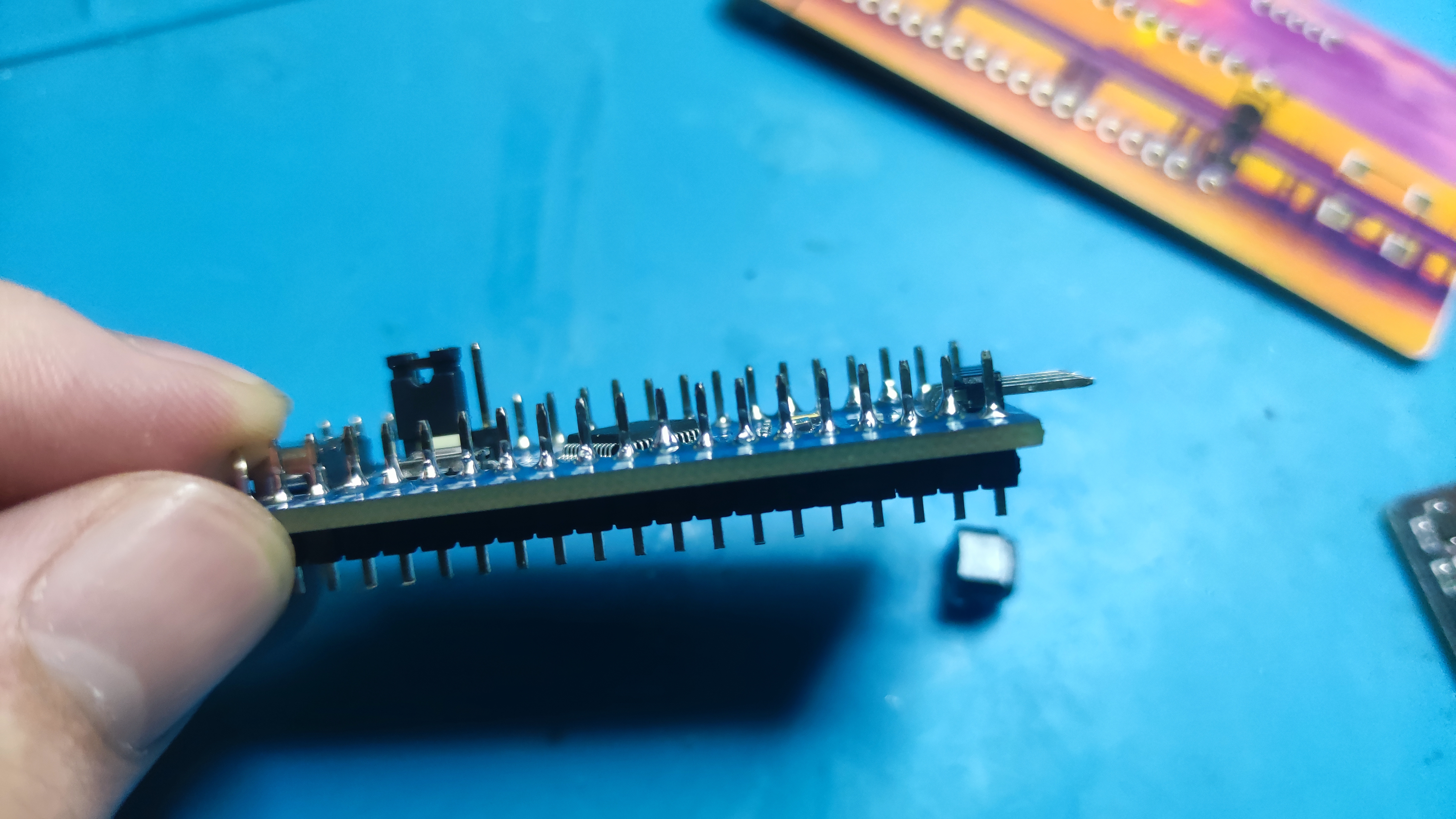 on top , soldering the CW32 last (a lesson learned the hard way). Pay attention to the positive and negative terminals of the button battery holder.
  Solder the OLED pin headers first, then solder the OLED, and
  finally solder the CW32
  . Shorten the boot pins and solder them together.
  Attach the model buttons to the buttons .
  Shorten the length of the toggle switch and
  assemble it flush with the panel. The complete assembly is shown in the image. The design wasn't fully considered; there weren't enough DuPont wire connectors, so they were directly soldered onto the board.
  Software


 京公网安备 11010802033920号

 SDB330


