I. Introduction
1. Appearance
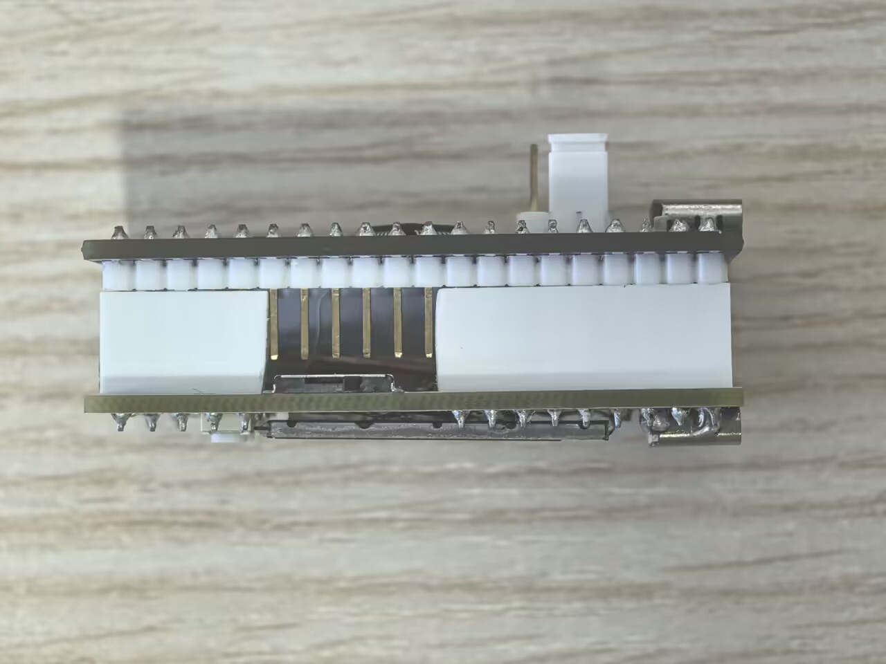
Based on the CW32F030C8T6 Earth Star development board, the small voltage and current meter is 2100mil (53.34mm) long, 900mil (22.86mm) wide, and about 2cm thick (excluding the boot0 header).

2. Functions
The screen can be lit without independently powering the development board (using MP2456GJ-Z), and the development board can be powered separately.
The current and voltage values are sampled at a frequency of 10 times per second, and the power is calculated. Since the power is always not very accurate, the power is not statistically analyzed. The voltage and
current are calibrated. The sampling rate does not need to be changed. The voltage and
current calibration is fixed. A total of 5 points are selected: the first (0) and the last (65535/maximum current and voltage) and the three points in the middle. After adjusting to the target value, the value is confirmed and saved to FLASH. 3.

Keypad:
Middle button (-): In non-adjustment mode, long press to switch between the main interface and the settings interface, short press to enter adjustment mode; in adjustment mode, long press to cancel the operation, short press to confirm or proceed to the next step.
Left button (↑) Right button (↓): In non-adjustment mode, long press to switch the settings page, short press to switch voltage levels on the main interface; in adjustment mode, both long and short presses are for adjustment, but the adjustment content is different.
II. Hardware Part
1. Dual Type-C female connectors: Input and output
are connected simultaneously using an FFC cable to connect the six pins D+, D-, CC1, and CC2, enabling fast charging support.

2. SSP9451 DC-DC step-down circuit (MP2456GJ-Z recommended):
4.2-40V input, 3.3V output, powering the CW32 development board. The schematic is drawn from the MP2451 datasheet.
The feedback voltage is 0.794V. Using resistor divider, the output voltage is 0.794/R1*(R1+R2). Taking R1=40.2kΩ and R2=124kΩ, the output voltage is approximately 3.243V ≈ 3.3V.
D2 prevents voltage leakage to VBUS when powered independently (refer to iDKMeter02C).

3. The voltage sampling circuit
uses a single-pole triple-throw switch for range switching, with three adjustable ranges. The range and 12-bit resolution are shown in the figure. The D5 Zener diode protects the chip pins.

4. The current sampling circuit
uses a 4mΩ sampling resistor, with both ends connected to an INA138 high-side current shunt monitor.
The INA138 common-mode voltage is up to 36V, capable of detecting unidirectional current (bidirectional models are too expensive). Reverse connection will not cause damage. The gain is configured via R10+R11, as shown in the formula. This circuit has a gain of 50V/V.
Pin 5 (V+) of the INA138 can be connected to 2.7~36V, and here it is powered by an independent 3V3 power supply.

5. Ripple measurement circuit (refer to iDKMeter02C):
C8 and R14 form a high-pass filter with a cutoff frequency of approximately 319Hz. R12 and R13 provide a 0.794V bias voltage.

6. SPI TFT screen & SPI 7. FLASH circuit

and button circuit:
Use a 100nF capacitor for hardware debouncing.

8. Development board pin assignment:
First, roughly assign the above circuits on the PCB, then refer to the CW32 datasheet (P26-27) to assign appropriate pins.
Hardware SPI: PB03, PB04, PB05 (SPI1)
SPI chip select and screen DC/RES: PA15, PB06, PA10, PA11
PWM output (BLK screen backlight): PA09 (GTIM3)
ADC: PA00 (IN0), PA07 (IN7), PB01 (IN9)
Buttons: PB07, PB08, PB09

9. PCB design
should be as small as possible, with the board outline matching the CW32 board size. Use 0402 packages for capacitors and resistors whenever possible. Cut some
Type-C female connectors, one on each side. Connect FFC to D+D-CC1CC2 to reduce the difficulty of wire routing
and ensure sufficient trace width for VBUS and GND (GND was previously copper-plated, but not this time; I forgot to do so and later added a copper trace).


10. Soldering & Assembly:
Soldering is somewhat difficult. First, solder the Type-C on the back of the screen, leaving the four mounting pins unsoldered. Then solder the two FFC connectors, apply solder paste, place components, and heat on the heating plate. Due to the colored silkscreen printing on the screen, it can only be heated once, and for a short time. After soldering the back, solder the Type-C on the front, reinforcing the four mounting pins. Then solder the buttons and adjacent capacitors. For the NMOS and current-limiting resistors in the screen circuitry, solder the headers
normally on the CW32 development board. The headers for the debugging interface do not need to be soldered. The female connectors on the sliding switch side of the voltage and current meter board need to be cut along with the plastic shell. For the female header, simply cut the pins
and solder the screen. The metal frame screen needs to be covered with transparent tape to prevent short circuits. Glue the back to the OCB.
Purchase a 5cm long FFC connector cable, cut both ends short, insert it into the connector and tighten. The CW32 development board's power input and voltmeter/ammeter input Type-C are on the same side; align the pin headers and female headers.
(If the ground wire is too thin, use a thicker copper wire)
. III. Software Part
1. Environment Configuration
: CLion is used for CW32 development. CLion has a beautiful interface and powerful functions. First, refer to the CLion configuration for STM32 development [Elegant Embedded Development] -- Zhihui has configured an STM32 development environment. A template project for CW32F030x8 is attached. You can also follow these steps to configure it (steps may be skipped; details can be found online or by referring to the template project).
1. After configuring the environment using the link above, create an STM32 project. Go to the project directory, back up the contents of the .idea folder, then change the chip in the project to STM32G030C8T6 (a chip with similar specifications and functions). Go back to the project directory, restore the .idea folder, and delete most files, keeping only the files in the [..idea], [.CoreStartup], and [.DriversCMSISCore] folders, and the [CMakeLists.txt] and [STM32xxx_FLASH.ld] files.
2. Then go to the CW32 official website, download the CW32F030 firmware library, and copy the contents of the [Libraries] folder to the [.DriversCMSISCW32F030_standard_peripheral] folder (the folder name is arbitrary). Copy the contents of 【ExamplesTemplateUSER】 to the 【.Core】 folder, and copy the files 【IdeSupportMDKWHXY.CW32F030_DFE.1.0.4.pack】 and 【IdeSupportEWARMarmconfigdebuggerCWCW32F030.svd】 to the project directory.
3. Locate the .s file in [.CoreStartup], rename it to startup_cw32f030.s, and open it. Compare it with the [IdeSupportMDKstartup_cw32f030.s] file in the firmware library. Modify the strings containing _Handler, except for the line commented out as Top of Stack. Follow the instructions in the .s file in the firmware library.
4. Locate the [.STM32xxxx_FLASH.ld] file, rename it to CW32F030x8_FLASH.ld, and open it. Refer to the datasheet (P28) and modify the RAM start address to 0x20000000, length to 8K, and the FLASH start address to 0x00000000, length to 64K.

5. Open the [.CMakeLists.txt] file and find include_directories(xxx). Change the STM32 library address to CW32 to include all the .h files added in the previous steps; the next line is add_definitions(-DDEBUG xxxx), comment it out with a # symbol; the next line file(xxx) also modifies the path to include all the .c files added in the previous steps; the next line set(LINER_SCRIPT xxx) changes the ld file name to the name from step 4; the next line adds add_link_options(--specs=nosys.specs) after add_link_options.
6. Right-click on the project panel, reload the CMake project, and then click Build. If there are no errors, the compilation is partially successful. The following are the download and debugging steps.
7. If you have Miniconda, you can create a new Python environment and download pyocd. If you don't have it and don't want to bother with it, you can directly download Python 3.7 and install it.
8. In the Clion run/debug configuration, add the native application, select pyocd.exe as the executable file, and the actual parameter is (can be modified appropriately): flash --target CW32F030C8 --pack=$ProjectFileDir$WHXY.CW32F030_DFP.1.0.4.pack $ProjectFileDir$cmake-build-debug$ProjectName$.hex
9. Add an embedded GDB server. The target remote is (can be modified appropriately) localhost:65533, the GDB server is pyocad.exe, and the actual GDB server parameter is gdbserver -p 65533 --pack=$ProjectFileDir$WHXY.CW32F030_DFP.1.0.4.pack --target CW32F030C8 -f 10M
10. Use the download or debug function (requires a downloader connection). Success is achieved if no errors occur. For debugging, select the [CW32F030.svd] file from the previous steps in the peripherals section (however, the register values are not visible; the reason is currently unknown).
2.
When writing the program, you need to refer to the CW32F030 datasheet, CW32F030 user manual, examples in the CW32F030 firmware library, datasheets for various devices, and search engines and AI
tools. However, using the firmware library seems less efficient than referring to the manual to operate the registers. The code I used varied depending on the time I wrote it, so it's a bit messy.
Memory region Used Size Region Size %age Used RAM: 4440 B 8 KB 54.20% FLASH: 60792 B 64 KB 92.76%
1.
Configure the PLL as the system clock using RCC. The PLL input reference clock is HSE (8MHz), multiplied by 8 to 64MHz. PCLK and HCLK are not divided (
refer to user manual P61). When switching the system clock, the FLASH control register FLASH_CR2.WAIT read wait period parameter needs to be configured synchronously: If the system clock frequency is not greater than 24MHz, the FLASH control register FLASH_CR2.WAIT should be set to 0; if the system clock frequency is greater than 24MHz, the FLASH control register FLASH_CR2.WAIT should be set to 1; if the system clock frequency is greater than 48MHz, the FLASH control register FLASH_CR2.WAIT should be set to 2.

2.
Refer to the ADC user manual (P435-P437). The CW32F030's ADC precision is 12 bits, and the ADC sampling time is 5/6/8/10 ADCCLK cycles. This project is configured with 10 cycles, and the successive approximation stage takes 19 ADCCLK cycles. A complete conversion requires 10 + 19 = 29 ADCCLK cycles. The maximum ADCCLK frequency is 4MHz at an internal 1.5V reference voltage and a 3.3V VDDA voltage. Setting it to the maximum is equivalent to PCLK. The 16-division frequency
is referenced in the user manual (P438). The CW32F030 has multiple ADC operating modes, including a single-channel multiple conversion mode that can achieve oversampling to 16-bit precision. Although this is not practically achievable, it is used as a mean filter (
refer to the user manuals (P441 and P458)). After configuration, start the conversion. After multiple successful conversions, ADC_ISR.EOA automatically becomes 1. The accumulated value can be read and cleared in the ADC interrupt. Switching channels will start the next conversion. To achieve 16 bits, 256 samples are required. Dividing the result by 16, the maximum single-channel full conversion frequency can be calculated as 4MHz/29/256 = 538.8Hz. For voltage and current sampling, the frequency is halved. This should be sufficient for this voltage and current meter. The code is too long to paste here (the project also includes ripple sampling, but the frequency is too low and it doesn't seem to have much effect, so I don't want to modify the code, and I'll leave it here).
3.
A total of three timers are used: BTIM1 is used for external triggering of ADC sampling with a period of 100ms; BTIM2 is used for button detection with a period of 10ms; and GTIM3 is used for PWM output to adjust the screen backlight brightness.
4. FLASH:
Originally, SPI FLASH was planned, but it seemed to be able to read but not write, and the problem was unclear. Therefore, the CW32's FLASH was used to store parameters
. Referring to the user manual (P111-) and datasheet, Page 127 (0x0000FE00-0x0000FFFF 512Bytes) was used to store parameters, supporting 8, 16, and 32-bit access. To facilitate directly obtaining the starting address of the parameter structure, 32 bits were written each time, making parameter reading simpler.


5. SPI:
SPI configuration is too simple to explain in detail. The FLASH chip is not used; the screen's CS pin remains pulled down, while the FLASH's CS pin remains pulled up.
The ST7735S screen driver is very simple, basically just modifying the driver code provided by the vendor. The command you might need to pay attention to is 0x36, as this command controls the screen's display orientation, refresh order, and whether the color scheme is RGB or BGR.

The basic display first uses the Address_Set function to send 0x2a and 0x2b commands to determine the display area (this area may be offset for screens from different manufacturers, which can be adjusted by adding or subtracting), then sends 0x2c to write to the memory, and then only needs to send the 16-bit color codes in sequence to display the colors according to the order specified by the 0x36 command.
6. The calibration function
consists of 4 arrays, two recording the ADC conversion values and two recording the corresponding current and voltage. Each array has 5 elements, with 0 at the beginning and 65535/maximum current and voltage at the end. After obtaining the ADC conversion value, it is converted. Values less than the first element are all 0.

7. The buttons and UI
are all implemented with a bunch of if switches and flag variables, which is very messy, but at least it is usable.
IV. Problems
1. The ground wire is too thin and the connection is a bit abstract.
2. Is the SSP9451 startup voltage a bit high? I'm not sure if it's a design issue, but the IN pin at 4.73V can't output 3.3V.
3. The INA138 offset voltage is ±0.2-1mV, less than 50mA (approximately, I don't have anything to measure).
4. The resistor design is entirely based on the 1.5V internal reference voltage, preventing the ADCCLK frequency from reaching its
maximum. 5. The three voltage measurement ranges are unnecessary and unused; if ranges are used, three sets of calibration data should be stored.
6. SPI FLASH write failed
. 7. I didn't have time to write the ripple function
. 8. In the calibration function, the starting point should sample more points and take the maximum value.
V. Project Attributes :
First public disclosure, original, no awards, no defense.
Open Source License: GPL 3.0
VI. Update
[v1.0] - 20240822
First Version


 京公网安备 11010802033920号

 AT27C010L-70TI


