Hardware Design
1. Power Supply Circuit
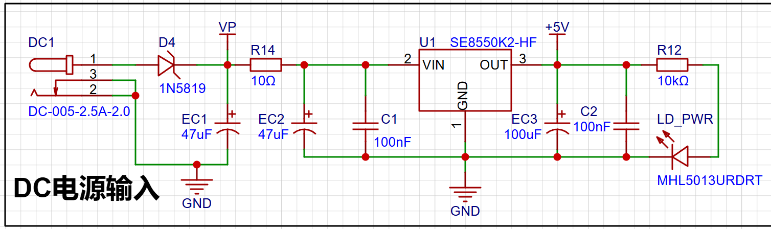
: LDO (Low Dropout Linear Regulator) Selection.
This project uses an LDO as the power supply. Considering that most voltmeter products are used in industrial scenarios with 24V or 36V power supplies, the SE8550K2 with a maximum input voltage of up to 40V was selected. The main reason for not using a DC-DC step-down circuit to handle the large voltage drop is to avoid introducing DC-DC ripple interference during the design process; a secondary reason is to reduce project costs.
When designing the DC plug, attention should be paid to the inner diameter of the DC socket. Common types include DC 2.1 and DC 2.5; ensure that the power connector and DC socket are compatible.
2. ADC Sampling Circuit:
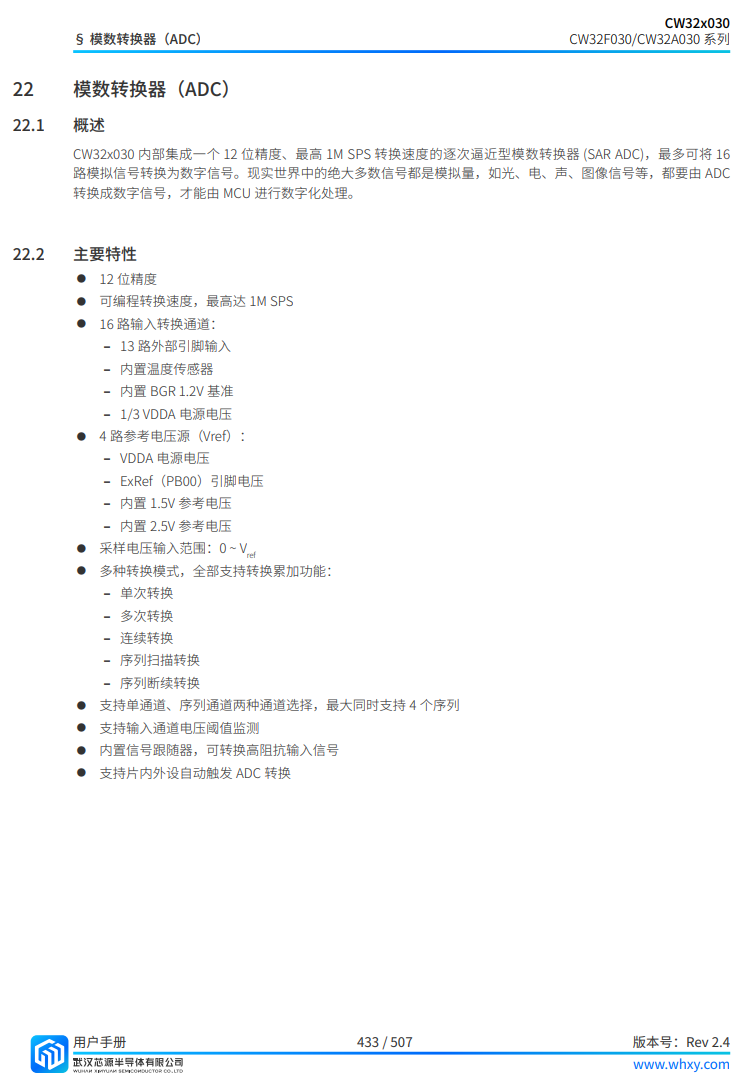
Advantages of CW32 in this Project
. Better ADC: 12-bit high-speed ADC, achieving ±1.0LSB INL 11.3ENOB, multiple Vref reference voltages... ... (STM32 only supports VDD=Vref).
Key characteristics of CW32's ADC.
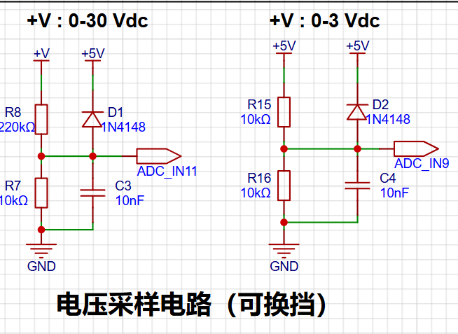
3. Voltage Sampling Circuit
: The voltage divider resistors in this project are 220K+10K, therefore the voltage division ratio is 22:1 (ADC_IN11).
The voltage divider resistor selection
is designed to measure the maximum voltage. For safety reasons, this project uses 30V (the actual maximum display value can be 99.9V or 100V).
The ADC reference voltage is 1.5V in this project, and this reference voltage can be configured through the program.
To reduce the power consumption of the sampling circuit, the low-side resistor (R7) is usually chosen as 10K based on experience.
Then, the high-side resistance of the voltage divider resistor can be calculated using the above parameters.
The required voltage division ratio is calculated, i.e., the ADC reference voltage. The input voltage is designed; using known parameters, 1.5V/30V = 0.05 can be calculated.
The high-side resistance is calculated as the low-side resistance/voltage division ratio; using known parameters, 10K/0.05 = 200K can be calculated.
A standard resistor is selected: a resistor slightly higher than the calculated value of 200K is chosen. We usually choose E24 series resistors; therefore, in this project, 220K, which is greater than 200K and closest to the calculated value, is selected.
4. Current Sampling Circuit
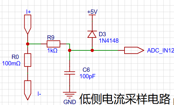
The sampling current designed for this project is 3A, and the selected sampling resistor (R0) is 100mΩ.
The selection of the sampling resistor mainly needs to consider the following aspects:
the maximum value of the pre-designed measurement current;
the voltage difference caused by the 3A current sensing resistor in this project; and
the power consumption of the current sensing resistor, which is generally not recommended to exceed 0.5V. A suitable package should be selected based on this parameter. Considering the power consumption (temperature) issue under high current, a 1W packaged metal-wound resistor was selected
. The voltage amplification factor of the current sensing resistor: No operational amplifier was used in this project to build an amplification circuit, so the factor is 1. The
current sensing resistance value can then be calculated using the above parameters. Selection:
Since no amplification circuit was used in this project, a larger sampling resistor was needed to obtain a higher measured voltage for measurement.
Considering that a larger resistor would result in a larger voltage difference and higher power consumption, a larger resistor cannot be selected indiscriminately.
A 1W packaged resistor was selected in this project, corresponding to a power rise of 1W.
Based on the above data, a 100mΩ current sensing resistor was selected in this project. According to the formula, 3A * 100mΩ = 300mV, 900mW.
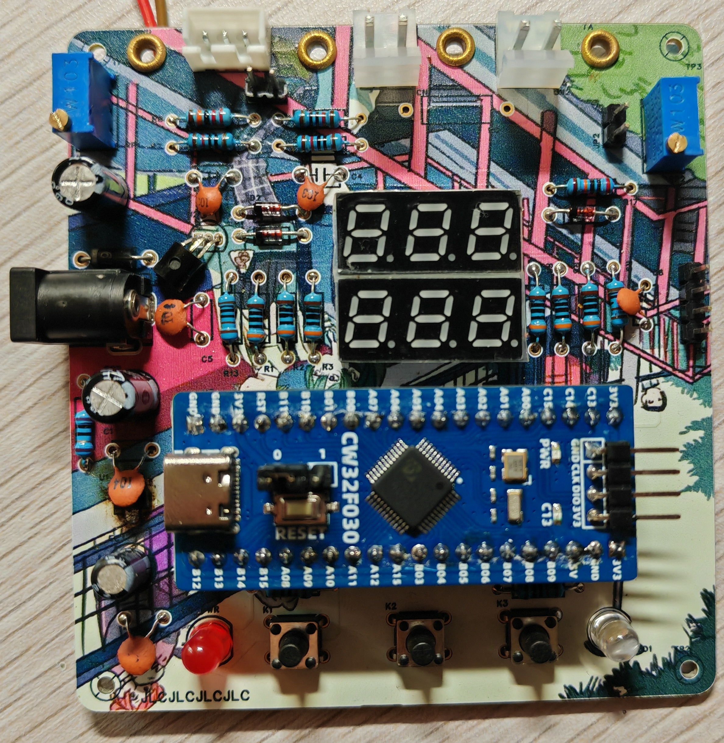
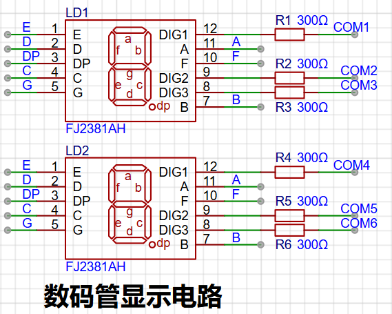
5. Digital Tube Display:
The driving principle of a digital tube mainly involves controlling the switching state of each LED segment to display numbers, letters, or symbols. The following is a detailed explanation of the driving principle:
Basic Structure of a Digital Tube:
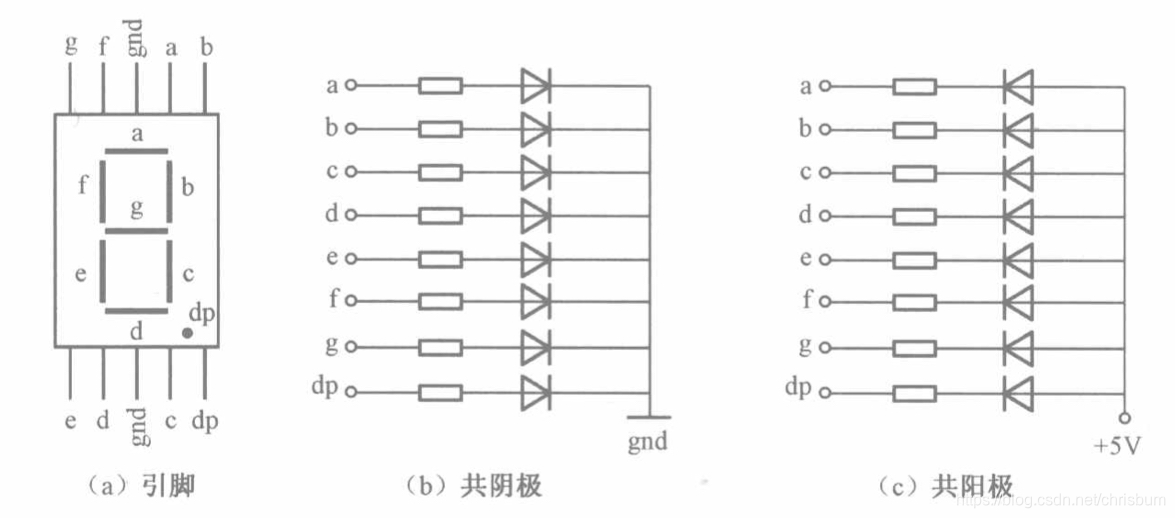
A digital tube typically consists of seven or eight LED segments (eight segments in this project). Each segment represents a part of the digital tube and can display numbers 0-9, letters AF, etc.
Digital tubes come in two types: common cathode and common anode. The difference lies in whether the common terminal COM (the end connecting all LEDs) is connected to the negative or positive terminal of the power supply.
Driving Methods:
Segment Selection: The desired number or character is displayed by controlling the switching state of each LED segment. Each segment corresponds to a control signal; when the control signal is on, the segment lights up, and vice versa. (a, b, c, d, e, f, g, dp)
Bit Selection: The digital tube to be displayed is selected by controlling the bit lines. Bit line control sets the bit line of the desired digital tube to a high level and the bit lines of other digital tubes to a low level. By continuously switching the state of the bit lines, the display switching between multiple digital tubes can be achieved.
Driving Circuit:
The digital tube driving circuit can be implemented through hardware circuits, such as using integrated circuits like digital signal processors (DSPs), microcontrollers (MCUs), or shift registers to generate control signals suitable for the LEDs.
These control signals can be in the form of pulse width modulation (PWM) signals, serial data signals, etc. By controlling the frequency, width, and amplitude of these signals, the brightness of the digital tube can be controlled, thereby displaying the desired numbers or letters.
Software Control:
In addition to hardware driving circuits, digital tubes can also be driven through software control. By programming to generate control signals suitable for the digital tubes, more flexible and complex display effects can be achieved, such as scrolling or alternating display of numbers.
Driving Common Cathode and Common Anode Digital Tubes:
For common cathode digital tubes, the common cathode pin is connected to the negative terminal of the power supply, and the control pin is connected to the output pin of the control chip. When a certain number needs to be displayed, the control chip outputs the corresponding encoded signal to the control pin, causing the corresponding LED segment to light up.
For common anode digital tubes, the working principle is similar to that of common cathode digital tubes, except that the common anode pin is connected to the positive terminal of the power supply, and the control pin is connected to the output pin of the control chip.
Encoding Display:
To display the corresponding numbers or characters on the digital tube, the segment data port must output the corresponding character encoding. For example, to display the number "0", the character encoding for a common anode digital tube is 11000000B (i.e., C0H), while the character encoding for a common cathode digital tube is 00111111B (i.e., 3FH). The specific encoding depends on the actual digital tube.
Dynamic and Static Display:
Digital tubes can use either static or dynamic display methods. In static display, each of the eight segments of each digital tube is connected to an 8-bit I/O port address. As long as the I/O port outputs a segment code, the corresponding character is displayed and remains unchanged. Dynamic display, on the other hand, lights up each digit of the digital tube one by one, achieving simultaneous visual display through rapid switching.
In summary, the driving principle of digital tubes is to control the switching state of each segment of the digital tube to display numbers, letters, or symbols, and to achieve display switching between multiple digital tubes through segment selection and digit selection. Furthermore, the driving of digital tubes can be implemented through hardware circuits or software control, and common cathode or common anode digital tubes can be selected for driving as needed.
This project actually uses dynamic scanning to drive the digital tube display.
Let's estimate the current required for the digital tube.
This project actually uses dynamic scanning to drive the digital tubes, so at any given time, only a maximum of 8 segments of the digital tubes (or LEDs) can be lit, or in other words, only one digit can be lit. According to the design, the required drive current is approximately 11mA (3.3V ÷ 300Ω ≈ 11mA) of the high-level voltage of the I/O port.
At this point, it's important to ensure that the selected MCU has sufficient current-source/current-sinking capability.
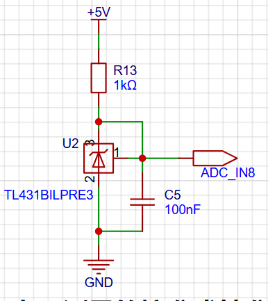
This project adds an extra TL431 circuit to provide a 2.5V reference voltage, which can be used to provide an external voltage reference for calibrating the AD converter. From a product design perspective, due to the inherent ADC performance advantages of the CW32, this circuit is not necessary. This circuit is designed on the development board to learn the relevant application principles.
The TL431 is a relatively "old" device, a classic, and widely used one, still found in many electronic products.
Many beginners may be encountering this device for the first time, so we will briefly explain its principles to help everyone better apply the TL431.
TI defines it as a "Precision Programmable Reference," and we can focus on several key characteristics on the first page of the references.
Precision: Precision indicates that its output voltage is very accurate. I used a TL431 with ±0.5% accuracy, which measured 2.495V on the board at room temperature. Compared to common Zener diodes, the accuracy is vastly different. In the application circuit diagram, the TL431 is represented by a Zener diode symbol.
Adjustable Output Voltage: The adjustable output voltage is between Vref and 36V. In our project, we use the output Vref voltage, which is approximately 2.5V. Therefore, we use 2.5V in the description, which is approximately equal to Vref.
Sinking Current Capability: This refers to how much current the output voltage pin can provide, which is greatly related to the resistance value (R13) in the application circuit. It should not be less than 1mA. If there is no need for sinking current, do not design the current to be too high, as this will cause unnecessary power consumption.
Digital voltmeter and ammeter with calibration function.zip
Panel_Panel_1_2024-08-21.epanm
CW32 voltmeter and ammeter housing. (zip)
test.jpg
Calibration Function.mp4
PDF_cw3 voltage and current meter.zip
Altium_cw3 voltage and current meter.zip
PADS_cw3 voltage and current meter.zip
BOM_cw3 Voltage and Current Meter.xlsx
92962
electronic


 京公网安备 11010802033920号

 2N6660_07


