This is a small, speed-adjustable fan with an atomizing humidifier and a dimmable light, built using the air001 chip and Arduino IDE programming.
It can achieve the following functions:
1. Free control of any module, allowing individual operation of one or two modules, or all modules to be on.
2. Individual potentiometers for controlling the brightness and speed of the light and fan.
Power Supply:
It uses DC 12V power (mainly because a suitable 5V fan is unavailable), and an internal LDO step-down regulator chip provides 5.0V power to the microcontroller and atomizer.
Application Scenarios:
1. Dimmable night light
2. Speed-adjustable fan
3. Humidifier.
Construction Process:
Circuitry: Originally, the plan was to directly use the MCU to output a 108kHz pulse to drive the humidifier, but it seems the MCU doesn't support this, causing a conflict with the PA5 pin and resulting in a blown tube. Therefore, the inductor was shorted, and the original atomizer interface was converted to a 5V power interface to power the external humidifier driver module.


Hardware: 12V fan, atomizing plate, and absorbent cotton swab.


wuhua_FS.zip
3D.zip
Demo.mp4
PDF_Fan with Atomizing Light and Speed Control.zip
Altium_Fan with Atomizing Light and Speed Control.zip
PADS_Fan with Atomizing Light and Speed Adjustment.zip
BOM_With Atomizing Light and Speed-Adjustable Fan.xlsx
94346
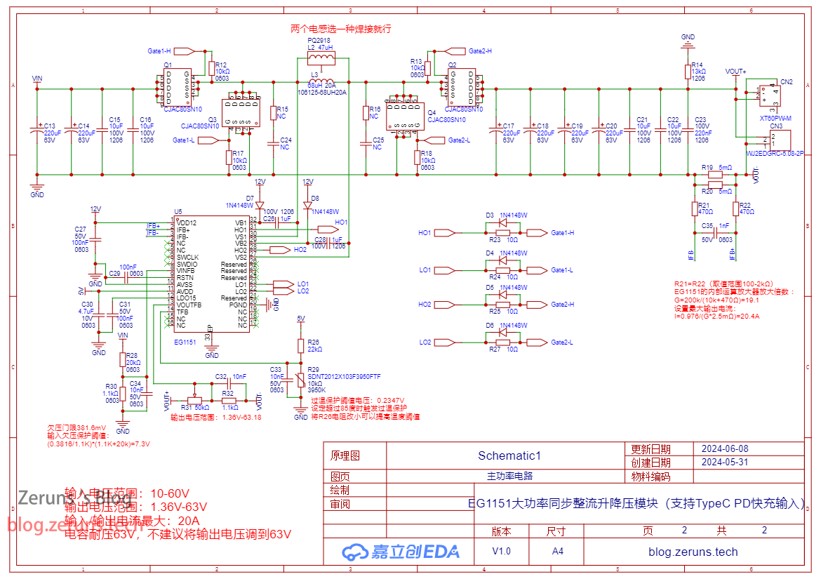
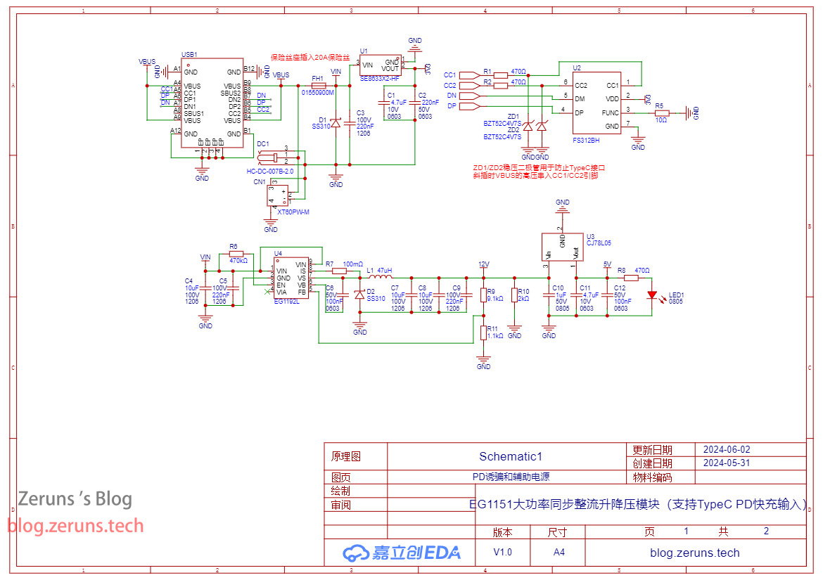
EG1151 Adjustable Buck-Boost Power Module (Supports Type-C PD Fast Charging Input)
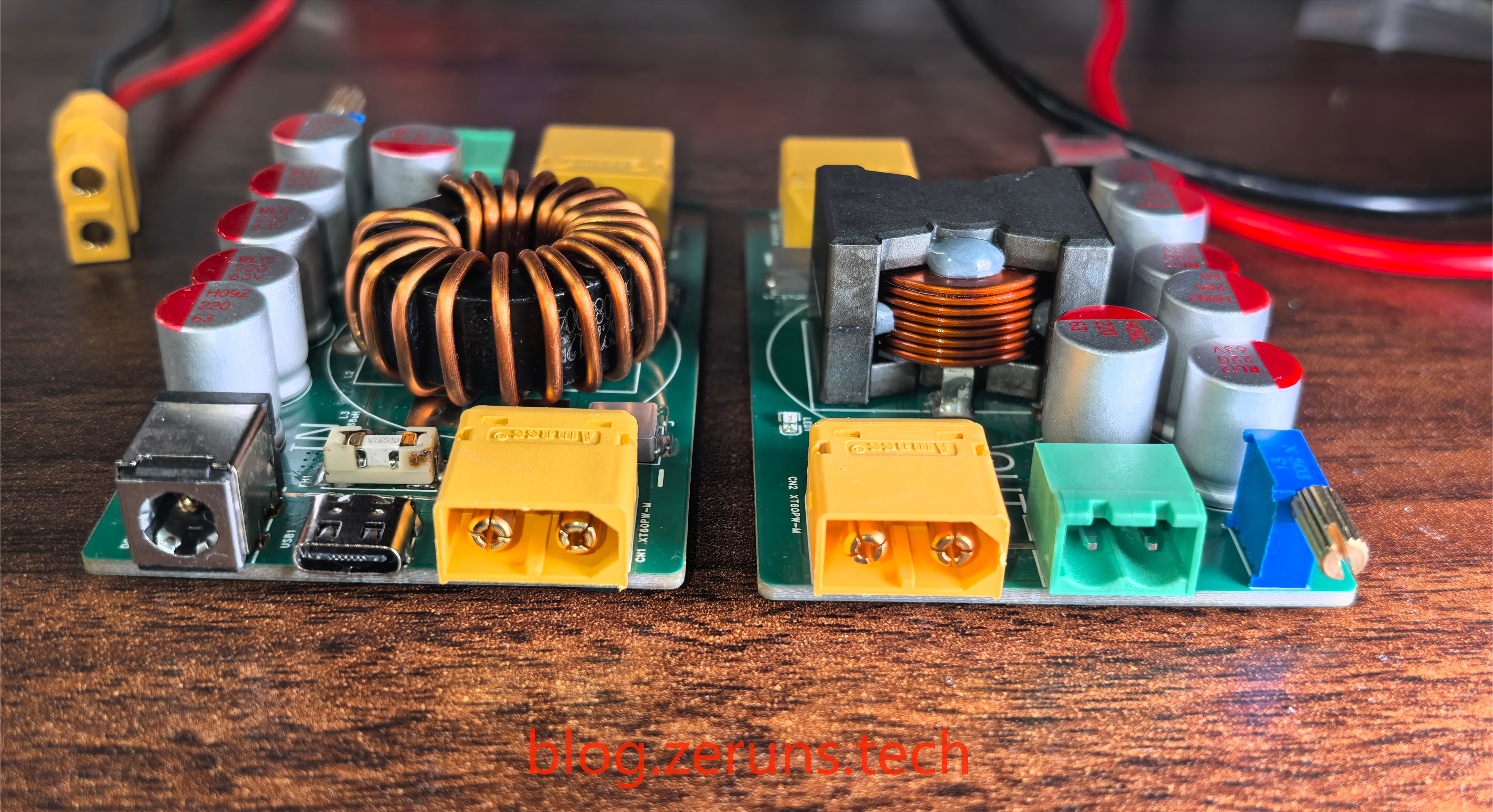
This high-power adjustable buck-boost DC-DC power module is based on the EG1151 chip. It supports Type-C interface input, PD3.1 spoofing with a maximum support of 48V, and also has XT60 and DC5.5 interface inputs. The maximum input/output voltage is 63V and the maximum input/output current is 20A.
This is an open-source, domestically produced high-power adjustable buck-boost DC-DC power module based on the EG1151 chip. It supports Type-C input, PD3.1 spoofing up to 48V, and also includes XT60 and DC5.5 input interfaces. The maximum input/output voltage is 63V, the maximum input/output current is 20A, and it supports overcurrent and overtemperature protection, with a maximum efficiency of 96.8%.
All components used in this module are domestically produced.
The PD3.1 spoofing chip used is the FS312BH, which can spoof a PD charger to output up to 48V. If the charger does not support this voltage, it will automatically select the closest voltage. For example, if your PD charger supports a maximum of 28V, it will output 28V. (As of the time of writing, it seems that most PD3.1 chargers on the market can only output up to 28V.)
To require a 28V Type-C input, besides the charger supporting PD3.1 28V, your data cable also needs to have an E-mark chip and support the PD3.1 ERP28V protocol.
Note: The three input interfaces cannot be used simultaneously; they are connected in parallel!
Video demonstration: https://www.bilibili.com/video/BV1fS411P7Cp/
Download link at the end of the article!
This module is designed for a maximum current of 20A, but in actual testing, it only reaches about 18A. At 18A, the voltage drop is already quite noticeable!
It's not great, so please don't criticize too harshly. If you have any suggestions for improvement, please leave them in the comments section. Friendly discussion is welcome.
Electronics/Microcontroller Technology Exchange QQ Group: 820537762
EG1151 Introduction:
The EG1151 is a four-switch buck-boost DC-DC power management chip. It integrates a reference power supply, oscillator, error amplifier, current limiting protection, short-circuit protection, half-bridge drive, and other functions. It can adopt corresponding control strategies based on the specific relationship between input and output voltages and different load conditions. It provides a stable voltage output across the entire fluctuation range of the input voltage. It is very suitable for applications requiring wide voltage range and high current boost/buck conversion, especially in situations where battery power voltage is not constant, and it also supports battery charging.
Features:
Wide input voltage range: 7V-150V;
High efficiency, up to 95%;
Undervoltage protection;
Over-temperature protection
; Supports battery charging;
Output short-circuit protection.
Package type: QFN32.
The actual product image


shows an aluminum shell purchased from Taobao, while the front and back covers were designed and 3D printed. 3D models of the shell and front/back covers are also included in the documentation. Regarding


chip soldering techniques:
The EG1151 chip is in a QFN32 package, and the FS312BH chip is in a DFN2X2-6L package. Both packages are very small and relatively difficult to solder, requiring some skill.
When soldering these two packages, if your PCB uses immersion gold plating, first apply solder to the pads; if it uses tin plating, apply solder to the chip pins. Note that it's best to use medium-low temperature solder (high temperature solder is difficult to use). Don't apply too much solder to the middle pads; just a little is enough, otherwise it will push the chip up and prevent the pins around it from making contact. If too much solder is applied, clean the soldering iron and slowly remove the solder, or use desoldering wick. After applying the solder, squeeze a little solder flux onto the pads, place the chip on them, and then place it on a heating plate or use a hot air gun. After the solder melts, gently move the chip with tweezers. If it automatically returns to its original position, it's done. After it cools down, check for any solder bridges. If there are any, repair them with a soldering iron.


Testing was performed
using an XT60 interface with a 24V input. The XT60 output interface was connected to a multimeter and an electronic load.

Using a Type-C input, a Cooltech 140W PD3.1 charger was connected, and it successfully induced 28V.

The maximum output is 63V.

Test equipment used:
HP 34401A 6.5-digit multimeter: https://blog.zeruns.tech/archives/772.html;
Ryton RD6012P digitally controlled adjustable power supply: https://blog.zeruns.tech/archives/740.html
; RIGOL DHO914S oscilloscope: https://blog.zeruns.tech/archives/764.html
; Juwei Electronics load: https://s.click.taobao.com/EdLEpkt. The highest efficiency obtained in the
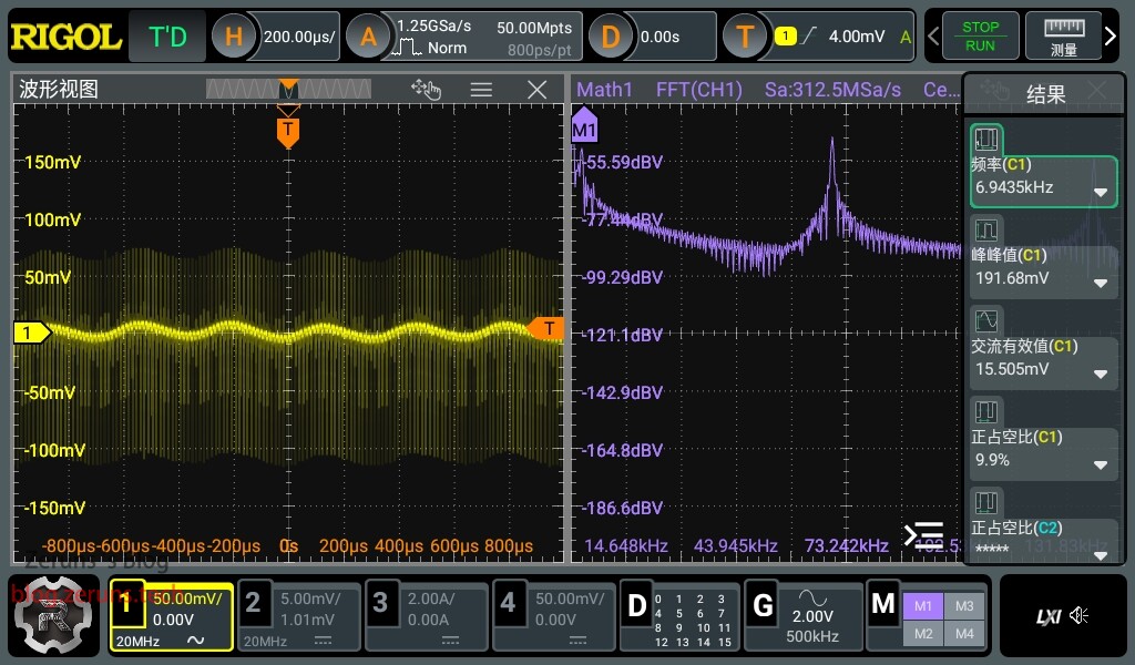
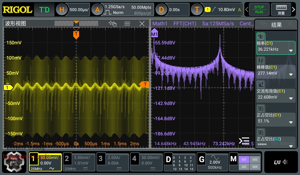
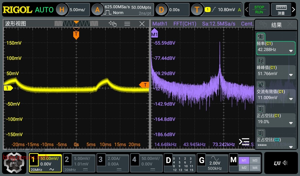
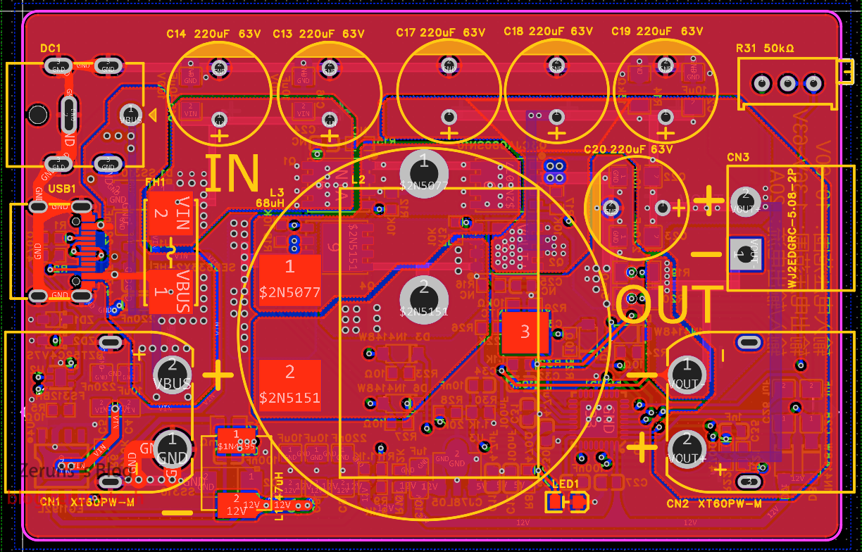
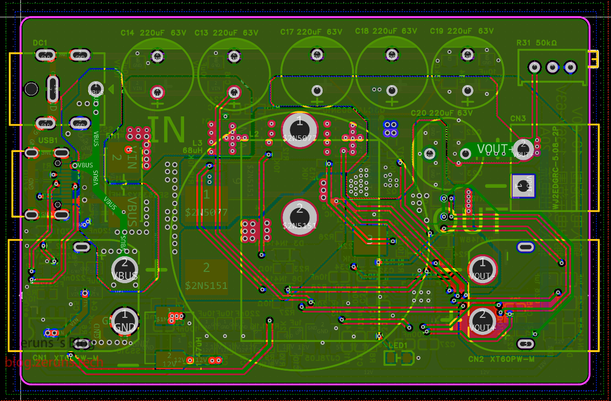
conversion efficiency test was 96.869%. The test data is shown in the table below: Input Voltage (V) Input Current (A) Input Power ( W) Output Voltage (V) Output Current (A) Output Power (W) Conversion Efficiency (%) 36.000 6.932 249.552 48.194 4.996 240.777 96.484 60.000 6.264 375.840 35.669 9.995 356.512 94.857 48.000 9.434 452.832 28.841 14.993 432.413 95.491 60.000 5.941 356.460 18.430 17.988 331.519 93.003 60.000 4.270 256.200 12.129 18.990 230.330 89.902 12.001 10.913 130.967 24.003 5.002 120.063 91.674 25.000 9.915 247.875 23.749
10.008
237.680
95.887
12.004
9.889
118.708
36.068
3.002
108.276
91.213
12.004
2.291
27.501
5.070
5.000
25.350
92.178
12.004
9.130
109.597
10.116
10.013
101.292
92.422
48.000 7.812
374.976
36.188
10.005
362.061
96.556
48.000
8.658
415.584
50.315 8.001 402.570 96.869 Ripple Test : The peak -to-peak ripple value for a 12V no-load output is approximately 32mV; the peak-to- peak ripple value for a 12V 10A no-load output is approximately 191mV; the peak-to-peak ripple value for a 12V 15A output is approximately 277mV; the peak -to-peak ripple value for a 36V no-load output is approximately 51mV; the peak-to-peak ripple value for a 36V 3A output is approximately 292mV; the peak-to-peak ripple value for a 60V no-load output is approximately 114mV; the peak-to-peak ripple value for a 60V 3A output is approximately 32mV. Schematic Diagram : Main Power Circuit; PD Decoy and Auxiliary Power Supply Circuit; PCB Top Layer; Inner Layer 1; Inner Layer 2; Bottom Layer; Component Purchase Addresses: Most of the components used in this project can be purchased here: 0603 Resistor and Capacitor Sample: https://s.click.taobao.com/SXT7pkt Type-C female connector 16P: https://s.click.taobao.com/vjLRskt EG1151 chip: https://s.click.taobao.com/le3gAkt EG1192L chip: https://s.click.taobao.com/pG2gAkt CJAC80SN10 MOSFET: https://s.click.taobao.com/aPsWWlt XT60PW interface: https://s.click.taobao.com/6jZ7pkt It is recommended to purchase components from LCSC's online store: https://activity.szlcsc.com/invite/D03E5B9CEAAE70A4.html Click on the BOM in the LCSC open-source link to immediately place an order on LCSC's online store; you can import the required components into your shopping cart with one click. Download links below include: LCSC EDA project, schematic PDF file, datasheets for various chips used, and 3D model files of the casing. Baidu Cloud download link: https://pan.baidu.com/s/1gNl48K25p6Pr3gi9lsyMAg?pwd=tmsv Extraction code: tmsv 123 Cloud download link: https://www.123pan.com/s/2Y9Djv-r3tvH.html Extraction code: 0cGK If you find this useful, you can tip me through the 123 Cloud links above. If it's a WeChat article (WeChat Official Account: zeruns-gzh), you can also click "Like Author" at the bottom of the article to tip me. Thank you. Other recommended open-source projects include: a three-phase power consumption data logger for easy monitoring of home electricity usage (https://blog.zeruns.tech/archives/771.html); an STM32F407-based LVGL project template (MSP3526 screen), including FreeRTOS and bare-metal versions (https://blog.zeruns.tech/archives/788.html); an STM32-based synchronous rectification Buck-Boost digital power supply (https://blog.zeruns.tech/archives/791.html); and the LM25118 automatic buck-boost adjustable DC-DC power module (https://blog.zeruns.tech/archives/727.html). EG1164 high-power synchronous rectification boost module open source, with a maximum efficiency of 97%: https://blog.zeruns.tech/archives/730.html 4G environmental monitoring node based on Zeruns Air700E (data on temperature, humidity, air pressure, etc.), uploading data to Alibaba Cloud IoT platform via MQTT: https://blog.zeruns.tech/archives/747.html Smart electronic load based on CH32V307 open source, an embedded competition entry open source: https://blog.zeruns.tech/archives/785.html


PDF_EG1151 Adjustable Buck-Boost Power Module (Supports Type-C PD Fast Charging Input).zip
Altium_EG1151 Adjustable Buck-Boost Power Module (Supports Type-C PD Fast Charging Input).zip
PADS_EG1151 Adjustable Buck-Boost Power Module (Supports Type-C PD Fast Charging Input).zip
BOM_EG1151 Adjustable Buck-Boost Power Module (Supports Type-C PD Fast Charging Input).xlsx
94348
F722 Dual-Gyroscope High-Voltage Flight Controller
A flight controller based on the STM32F722RET6, featuring a built-in high-voltage BEC, supporting a voltage range of 3-10 seconds, dual ICM42688 gyroscopes, and supporting X8 mode.
I. Product Introduction This
is a drone controller based on the STM32F722RET6 microcontroller.
This module is the flight control board and can be used with various electrical systems to achieve low-cost drone operation.
II. Application Scenarios
Primarily used for small quadcopter drones; suitable for X8 racing drones.
III. Product Overview
This low-cost F722 drone controller
uses the high-performance STM32F722RET6 (216MHz) microcontroller from the STM32F7 series. It can be configured to 240MHz via the CLI interface
and employs a dual IMU design (dual ICM42688P) for stable flight. This makes flight more stable and control more precise, allowing for easy control whether in racing or free flight at full speed. It also supports replacement with an LGA-14 packaged gyroscope.
Built-in 5V/4A and 9V/4A BEC provide stable and reliable power to external peripherals such as GPS, optical flow meter, receiver, magnetometer, and image transmission devices.
Dual LDOs (SP6205 @500mA), one of which provides dedicated power to the IMU for more stable gyroscope operation. It also supports replacement with SOT-23-5 packaged LDOs. The SPX3819's
built-in OSD module is recommended, allowing real-time display of aircraft data on the video transmission interface for easier pilot control.
An integrated DPS-310 high-performance barometer provides real-time altitude sensing.
Onboard SBUS inverter and active buzzer driver are included.
Multiple interfaces are provided for easy connection to various peripherals. UART: 7 channels (1, 2, 4, 5, 6) SBUS: 1 channel (RX3) I2C: 1 channel PWM: 8 channels USB: (Type-C)


IV. Product Parameters
Main Controller (MCU): STM32F722RET6
Gyroscope (IMU)
: ICM42688P+ICM42688P (SPI1) Character Overlay (OSD
): AT7456E (SPI2) Barometer: DPS-310 (I2C1
) Black Box: W25Q128JVPIQ (SPI3)
Input Voltage: 3-10S (10-44V)
Output Voltage: BEC-9V-4A (LC Filter) BEC-5V-4A
Buzzer: Supports 5V active buzzer
Supported Firmware: INAV Betaflight
Dimensions: 38.5mm x 38.5mm,
Hole Spacing: 30.5mm x 30.5mm,
USB Type: TYPE-C,


STM32F722RET6 microcontroller,
AT7456E OSD overlay chip,
DPS310 barometer ,
dual ICM42688P gyroscope
sensor, independent power supply,
128M black box
MCU power
supply, ESC terminals, silkscreened “GB5678RC” meaning “GND,VBAT,M5,M6,M7,M8,RX5,CURR”, pay attention to the wiring sequence when wiring, ESC
terminals, silkscreened “GB1234RC” meaning “GND,VBAT,M5,M6,M7,M8,RX5,CURR”, pay attention to the wiring sequence when wiring,
9V BEC power supply, maximum output current 4A, with LC filter, lower ripple
9V The BEC power supply uses an SMB-packaged TVS diode with a maximum output current of 4A
. For 6S voltage, an SMBJ30CA diode can be soldered; for 10S voltage, an AMBJ48CA
dual-channel current meter fusion adder chip can be soldered to add the two current meters together.
The BOOT button,
TYPE-C interface
, and GPS interface are marked "SD,SC,R4,T4,5,G", meaning "SDA,SCL,RXD4,TXD4,+5V,GND". Pay attention to the wiring sequence when connecting
. The DJI interface is marked "SB,G,R2,T2,G,+9V", meaning "SBUS,GND,RXD2,TXD2,GND,+9V,". Pay attention to the wiring sequence when connecting.
V. Usage Instructions
: Firmware Burning: Press and hold the BOOT button, connect the flight controller USB to the computer, release the BOOT button to enter DFU mode. Then use Betaflight Configurator or other ground stations to burn the firmware. For INAV firmware burning, please use the INAV ground station. (Firmware attached)
If it's INAV firmware, the next steps involve configuration and parameter tuning on the ground station. If it's BF firmware, you'll also need to flash a specific configuration file via the CLI command line. (BF configuration file attached)
VI. Notes
: Several points to note during the creation process:
Replicating this project is quite difficult. The smallest component uses a 0402 package, which is challenging to solder. It requires exceptional patience (potentially requiring multiple debugging sessions, or even crashes), as well as strong learning abilities and the capacity to solve problems through various methods, including but not limited to soldering, firmware flashing, and proper firmware usage. Therefore, this project is only recommended for model enthusiasts who have experience with drones, are skilled at soldering surface-mount components, and have some understanding of PCBs and components. Please carefully consider your hands-on and problem-solving abilities before deciding whether to replicate this project.
Power Supply Voltage Selection: The theoretical maximum input voltage for this flight controller is 60V. To allow for a margin of safety, it is recommended to use 3-10s model aircraft batteries or 18650/21700 battery packs for power supply. The image transmission voltage is controllable and requires PINIO configuration.
Component Selection: Filter capacitors need to be selected based on the input voltage (it is recommended to purchase capacitors from LCSC; Taobao often has issues with falsely advertised specifications, and more common capacitors can be purchased from a certain Taobao seller).
When soldering, please use silicone wire (28-30AWG) to connect the flight controller to prevent the solder pads from detaching under stress.
It is recommended to use hot melt glue to secure the six 10-pin SH1.0 connectors after soldering to prevent the solder pads from detaching under stress.
Pay attention to the wiring sequence! Pay attention to the wiring sequence! Pay attention to the wiring sequence!
The total component cost for this project is approximately 80 RMB. However, note that the flight controller cost often only accounts for a small portion of the overall drone cost.
Open source license: CC-BY-NC-SA 3.0, Creative Commons Attribution-NonCommercial-ShareAlike.
The flight controller is compatible with HAKRC F722V2 firmware. If the IMU cannot be recognized, please select the "Core Only" option during flashing.
The current meter uses an op-amp for addition, dividing the two current meter readings by 2 before adding them together. This results in a dead zone and inaccuracy in the current meter readings. Note that
the flight controller design is based on the Chongshan ST32 standard version. Permission has been obtained from the author, Xiao An.
CC: Abbreviation for Creative Commons license.
BY: Attribution. You must give appropriate attribution, provide a link to this license, and indicate whether modifications were made (to the original work).
NC: Non-Commercial. You may not use this work for commercial purposes.
This design is provided "as is" without any guarantee of employment or warranty, and we are not liable for any damage or loss to the creator or any third party's person or property caused by product design, improper operation, or violation of local laws and regulations.
VII. Test Video
The video demonstrates the testing of the built-in onboard IMU, barometer, OSD, and external GPS when the flight controller is connected to the BF ground station after being connected to the computer.
// Please see the attachment for the demonstration video .
VIII. Real Photos


Please download the attached source file. Opening it with an editor may result in errors (as it is directly copied), so please download and open the attachment.
Demo video.mp4
Source file .epro
Demo video 2.mp4
PDF_F722 Dual Gyroscope High-Voltage Flight Controller.zip
Altium_F722 Dual Gyroscope High-Voltage Flight Controller.zip
PADS_F722 Dual Gyroscope High-Voltage Flight Controller.zip
BOM_F722 Dual Gyroscope High-Voltage Flight Controller.xlsx
94349
The Book of Answers (audio available)
The "Answer Book" is a microcontroller-based application; pressing a button refreshes the screen text and plays the corresponding audio.
This is a "Book of Answers" program based on an STC microcontroller. Pressing a button refreshes the screen text and plays the corresponding audio. The code is a version without music; to play music, you need to buy a mini MP3 module, connect it, and add this code.
/******************************************************************************- Functionality: Enables the chip to play the first and second tracks upon power-up. A basic program is provided for user testing. - Date: 2013-05-06 - Operating Environment: STC crystal oscillator: 11.0592MHz, baud rate: 9600 - Note: Debugged successfully on the Puzhong Technology 51 development board --- STC89C516RD+1. This test program requires a device to be online in the module or chip solution, such as a USB flash drive, TF card, or FLASH. ******************************************************************************/
#define COMM_BAUD_RATE 9600 // Serial port baud rate #define OSC_FREQ 11059200 // Running crystal oscillator: 11.05926MHZ
static unsigned char Send_buf[10] = {0}; /*void Delay_Ms(unsigned int z){unsigned int x=0 , y=0;for(x=110 ; x>0 ;x--)for(y=z; y>0;y-- );}*//**************************************************************************************- Function description: Serial port 1 initialization - Note: Set to 9600 baud rate ******************************************************************************/void Serial_init(void){//TMOD = 0x20; // Set T1 as baud rate generator//SCON = 0x50; // 0101,0000 8 data bits, No parity //PCON = 0x00; //PCON=0; //TH1=256-(OSC_FREQ/COMM_BAUD_RATE/32/12);//Set to 9600 baud rate //TL1=256-(OSC_FREQ/COMM_BAUD_RATE/32/12);//TR1 = 1; //Timer 1 enabled //REN = 1; //Serial port 1 receive enabled //ES = 1; //Serial port 1 interrupt enabled PCON &= 0x7F; //Baud rate not multiplied SCON = 0x50; //8-bit data, variable baud rate AUXR |= 0x40; //Timer clock 1T mode AUXR &= 0xFE; //Serial port 1 selects Timer 1 as baud rate generator TMOD &= 0x0F; //Set timer mode TMOD |= 0x20; //Set timer mode TL1 = 0xD9; // Set the initial value of the timer TH1 = 0xD9; // Set the reload value of the timer ET1 = 0; // Disable timer interrupt TR1 = 1; // Start timer 1}
void Uart_PutByte(unsigned char ch){SBUF = ch;while(!TI){;}TI = 0;}/******************************************************************************- Function Description: Send commands out of the serial port [including control and query] - Parameter Description: CMD: Represents control commands, please refer to the command table, which also includes related query commands feedback: Whether a response is required [0: no response required, 1: response required] data: Parameters to be transmitted **********************************************************************************/void SendCmd(unsigned char len){unsigned char i = 0 ;Uart_PutByte(0x7E); // Start for(i=0; i{Uart_PutByte(Send_buf[i]) ;}Uart_PutByte(0xEF) ;//End}/******************************************************************************- Function Description: Sum Check - The idea of sum check is as follows: The sent command removes the start and end. The middle 6 bytes are accumulated and finally the inverse code is taken. The receiving end removes the start and end of the received frame of data. The middle data is accumulated and the received check byte is added. It is exactly 0. This means that the received data is completely correct. ******************************************************************************/void DoSum( unsigned char *Str, unsigned char len){unsigned int xorsum = 0;unsigned char i;for(i=0; i{xorsum = xorsum + Str[i];}xorsum = 0 -xorsum;*(Str+i) = (unsigned char)(xorsum >> 8);*(Str+i+1) = (unsigned char)(xorsum & 0x00ff);}void Uart_SendCMD(unsigned char CMD ,unsigned char feedback , unsigned char dat){Send_buf[0] = 0xff; // Reserved bytes Send_buf[1] = 0x06; // Length Send_buf[2] = CMD; // Control instructions Send_buf[3] = feedback;// Whether feedback is needed Send_buf[4] = (unsigned char)(dat >> 8);//datahSend_buf[5] = (unsigned char)(dat); //datalDoSum(&Send_buf[0],6); // Verify SendCmd(8); // Send this frame data}
IMG_20240101_172516.jpg
video_20240101_172007.mp4
The Book of Answers.c
STC8.h
PDF_The Answer Book (with audio).zip
Altium_The Book of Answers (with audio).zip
PADS_The Book of Answers (with audio playback).zip
BOM_The Book of Answers (audio can be included).xlsx
94350
RTL8812EU baseplate OPENIPC_FPV
The B-Link 8812eu network card soldering base plate measures 38*38mm and can be directly screwed onto modules such as the MC800S for use in open-source high-definition video transmission projects like OpenIPC. A 26*26mm heatsink is recommended for the recessed slot.
This design references the 8812EU network card soldering baseboard by Lin Hai Network Card expert: https://oshwhub.com/zcshanlin/8812eu-di-ban. Based on this, the pin positions of the 8812eu schematic were modified, and a 26*26mm heatsink and a 1.25mm socket were used.
PDF_RTL8812EU baseplate OPENIPC_FPV.zip
Altium_RTL8812EU baseplate OPENIPC_FPV.zip
PADS_RTL8812EU baseplate OPENIPC_FPV.zip
BOM_RTL8812EU baseplate OPEIPC_FPV.xlsx
94351
VORON 2.4 TAP 5-24V verified
Based on the open-source VORON TAP circuit board, the photoelectric sensor was redesigned and replaced with the EE-SX398, which is cheaper, costing less than 10 yuan per unit, and supports a wide voltage range of 5-24V.
Project Description:
The VORON TAP is a leveling sensor based on a photoelectric sensor. It boasts high precision while maintaining an attractive appearance, and also functions as a collision protection switch. It is currently the most commonly used leveling sensor for VORON 2.4. This design is a redesign based on the open-source VORON TAP circuit board, supporting a wide voltage range of 5-24V. Replacing the photoelectric sensor with an EE-SX398 reduces costs, with a single sensor costing less than 10 RMB. Some users have reported occasional burnout of this step-down chip under power; therefore, a 1-ohm resistor is added to the input to effectively solve this problem. Alternatively, this resistor can be replaced with a diode to add reverse connection protection.
Schematic,

PCB Design,

Physical Demonstration, Notes:

The
10uf capacitor is a filter capacitor at the power input. If using 24V, it is recommended to purchase a 50V capacitor.
Other Attachment Upload
Instructions: Entries participating in this event must upload all project-related program attachments to the open-source platform or personal code storage cloud. The maximum upload size for attachments is 50MB (please do not upload to the LCSC workspace, as there are limitations).
Welding Assistance.html
PDF_VORON2.4 TAP 5-24V verified.zip
Altium_VORON2.4 TAP 5-24V verified.zip
PADS_VORON2.4 TAP 5-24V verified.zip
BOM_VORON2.4 TAP 5-24V verified.xlsx
94352
Taishanpai Charging Expansion Board
(Open Source) Newly made Taishanpai casing, battery-powered, serial port board + charging board + 3.1 screen board
https://oshwhub.com/tt_708/tai-shan-pai-chuan-kou-kuo-zhan-ban
(Open source) Newly manufactured Taishanpai battery pack for power supply.


IMG_0861.mov
PDF_ Taishanpai Charging Extension Board.zip
Altium_Taishanpai Charging Expansion Board.zip
PADS_Taishanpai Charging Expansion Board.zip
BOM_ Taishanpai Charging Expansion Board.xlsx
94353
Low-cost USBASP-compatible AVR programmer based on CH552
This project is based on the picoAVR project on Github, is compatible with USBASP and SerialUDPI, and supports programming AVR microcontrollers through common ISP and UDPI interfaces, at a low cost.
Updated 2024/06/07: The programmer has been verified to use avrdude to program AVR microcontrollers under Linux.
Note: Do not trust the BOM automatically generated by the system; please refer to the parameters in the schematic diagram
. As the title suggests, this project is an ultra-low-cost USBasp compatible programmer based on the WCH CH552G microcontroller, providing AVR-ISP and UDPI programming interfaces.
This project mainly modifies the original project as follows:
The microUSB interface is replaced with the more common USB-TYPE-A interface;
the LDO is replaced with a higher current SPX1117M3.3 (compatible with AMS1117-3.3, requires modification of the filter capacitor)
; the voltage switch is replaced with a common pin header + jumper cap.
Programming steps:
Short the boot jumper, insert the programmer into the computer,
open WCH ISP Studio, select "E8051USB Series (CH54X/CH55X)" in the "MCU Series View,"
select "Target Program 1" (the firmware provided in the attachment), and set the chip configuration according to the screenshot
to start programming. After programming is complete, disconnect the boot jumper. A picoAVR device should appear in Device Manager > Universal Serial Bus devices.

The hardware has been verified, but the software still has some issues. The author's device name is inconsistent with the original, and avrdude does not recognize the device. It is recommended not to attempt a replication for now.
The programmer can normally program AVR microcontrollers under Linux using avrdude. For Windows platforms, avrdude still cannot recognize the device (common USBasp programmers can, all of which use the libusb-win32 driver built by zadig). I am currently communicating with the original author on a GitHub issue and trying to resolve the issue. Anyone with ideas is welcome to join the discussion. Currently, it is advised to proceed with caution when recreating the project.
Original project address: https://github.com/wagiminator/AVR-Programmer/tree/master/picoAVR_Programmer
picoavr.bin
PDF_Low-Cost USBASP Compatible AVR Programmer Based on CH552.zip
Altium CH552-based Low-Cost USBASP Compatible AVR Programmer.zip
PADS_CH552-based Low-Cost USBASP Compatible AVR Programmer.zip
BOM_Low-Cost USBASP Compatible AVR Programmer Based on CH552.xlsx
94355
XT60 boost/buck converter
Suitable for temporary emergency use, using LM2596S and XL6019 modules or XL4016 and (search 8A boost module on Taobao).

PCB.rar
Finals Code.rar
Preliminary round code.rar
PDF_XT60 boost/buck converter.zip
Altium_XT60 boost/buck converter board.zip
PADS_XT60 boost/buck converter board.zip
BOM_XT60 boost/buck converter.xlsx
94356
USB Type-C SS 2.5G Ethernet Card RTL8156B
A 2.5G Ethernet card with a USB Type-C port using the RTL8156B-CG chip.
Please note that this project is for personal learning and sharing purposes only. It is not recommended to adopt this solution to reduce costs. This solution has not undergone professional verification and inspection. I do not have the datasheet and official design schematic for the RTL8156 chip, and there may be several unknown issues and faults. Stability needs further consideration. Compared to products with the same chip currently on the market, this project is neither cheap (costing approximately 35 RMB) nor stable, and there is no after-sales service. Please weigh the pros and cons carefully before DIYing solely for the sake of "cheapness." Thank you!
Updated 2024.6.7: Please read Part Twelve.
Project discussion group (QQ): 753341673
I. Acknowledgements
This project references and modifies existing projects:
https://oshwhub.com/aknice/rtl8153b
(referencing the USB Type-C switching part of this project)
https://oshwhub.com/vvwall/tao_net
(referencing the 2.5G Ethernet part of this project).
Thanks to the two contributors for their open-source contributions, which made this project possible!


II. Project Status:
Some functions of this project have been verified and can be built directly, but there will be some problems.
Currently, the network card's receiving speed is basically up to 2.37Gbps,
but the sending speed has issues, only reaching 1.44Gbps (resolved).
Test environment: Two computers, both running Windows 10, one a 2016 Mac using the network card from this project, and the other an ASUS B550 5800X combination using the onboard Intel I225-V network card.
Throughput testing was performed using iPerf3
(updated 2024.6.7).
After driver correction,
the network card's receiving and

sending commands were tested.

The network card's receiving
command was: `iperf3 -c 192.168.50.21 -p 8888 -t 20 -O 3` (all commands were entered on the ASUS machine; the network card in this project acts as the server).

The network card's sending
command was: `iperf3 -c 192.168.50.21 -p 8888 -t 20 -O 3`. -R

for multi-threaded receive, command: iperf3 -c 192.168.50.21 -p 8888 -t 20 -O 3 -P 16

Multi-threaded send, command: iperf3 -c 192.168.50.21 -p 8888 -t 20 -O 3 -R -P 16

The currently suspected causes of the fault are as follows (resolved):
1. For convenience, this project used an integrated network interface transformer component (HR911130A) that could only operate at 1Gbps speed.
2. For ease of soldering, the USB 3.0 circuitry in this project used coupling capacitors with a 0603 package size
. 3. There may be unknown issues with the wiring.
III. Operating temperature:
After a continuous 1-minute receive/transmit test, the surface of each chip and the front and back surfaces of the PCB felt warm. At
a room temperature of 22.3 degrees Celsius
, iPerf3 was used to send multi-threaded stress test
commands: `iperf3 -c 192.168.50.21 -p 8888 -t 20 -O 3 -R -P 32`.
The infrared temperature recorded on the front (chip side) around the 50th second of the stress test was 40.1 degrees Celsius.

The infrared temperature recorded on the back (around the 54th second of the stress test) was 37.8 degrees Celsius.

IV. Impedance Matching:
The 4-layer board with a stack-up structure of JLC process, JLC04101H-3133 (1.0mm board thickness),
is calculated using the official JLC impedance calculator as follows: (https://tools.jlc.com/jlcTools/index.html#/impedanceCalculatenew)
For the USB 2.0 section, a differential impedance of 90 ohms is used, resulting in a line width of 6.2mil and a spacing of 8mil.
For the USB 3.0 section, a differential impedance of 95 ohms is used, resulting in a line width of 5.5mil and a spacing of 8mil.
For the MDI section, a differential impedance of 100 ohms is used, resulting in a line width of 5.2mil and a spacing of 10mil
. V. Schematic Diagram:

VI. PCB Diagram:
Top Surface,

Inner Layer 1,

Inner Layer 2,

Bottom Surface

VII. Power Supply Diagram: VIII.

Partial Component Price Reference:
RTL8156B-CG 25 RMB
, VL162 3 RMB,
HR911130A 5 RMB (possibly counterfeit),
Used USB Type-C SuperSpeed Data Cable 16 RMB
IX. Partial Design Reference:
VL160: https://www.via-labs.com/product_show.php?id=72
VL162: https://www.via-labs.com/product_show.php?id=106
VL162 Reference: https://blog.csdn.net/weixin_54493972/article/details/119379313
X. Production Suggestions:
Please do not use the BOM automatically generated by the JLC system or directly perform SMT, as they are inaccurate. Please refer to the attribute values in the project file. I have also uploaded my own BOM for reference (it may contain errors, please double-check).
The design documents for this project are suitable for 4-layer boards using JLC technology, with a stack-up structure of JLC04101H-3133 (1.0mm board thickness), and impedance control within 20%.
The USB-C female connector can only be installed on PCBs with a board thickness of 1.0mm or less.
The tantalum capacitor in the output capacitor that steps down to +0.95V is optional.
All capacitors except tantalum capacitors must be installed, and the capacitance of the 1206 capacitors cannot be too small.
When soldering QFN chips, place a small amount of solder (about the size of a grain of rice) on the center GND side, and use slightly more solder around the edges to ensure the solder wets the chip leads. After mounting the chip on the front, use a heated soldering station. Finally, use a soldering iron and flux to remove excess solder around the edges.
Please note that QFN chips are very prone to cold solder joints; it is recommended that inexperienced users practice soldering using other scrapped chips first.
After completing the front-side component placement, use a bracket to flip the PCB board and continue with the back-side component placement. Back-side soldering should be done using a hot air gun. For integrated hot air guns, select 360 degrees and 30% airflow, preheat first, then target specific areas for soldering.
Please note that when soldering the back side, do not allow front-side components to touch other objects and shift.
After soldering, clean the flux using a reputable brand-name cleaning agent. A relatively large amount may be needed. Except for plastic parts such as connectors, you can directly soak the components in the cleaning agent for cleaning. After cleaning, actively wipe the cleaning agent dry with a paper towel or lint-free cloth; do not wait for it to evaporate on its own to avoid residue.
XI. Future Outlook
: Adding ESD/TVS protection devices to the USB interface accessories
; optimizing cabling;
and replacing the wiring with RJ45 connectors and network transformers compliant with 2.5G and above standards.
XII. Subsequent Updates
(June 7, 2024):
1. The issue of the network card's transmission speed not meeting the standard has been successfully identified. The main cause was a problem with the Windows network card driver on the test computer. For details, please see https://www.acwifi.net/21188.html and https://www.bilibili.com/video/BV1pS4y1p7qS. The above two web pages and videos basically confirmed that it was a network card issue. After correcting the driver to version 10.54.608.2022, the transmission speed returned to normal. The driver has been uploaded as an attachment. Please note that this driver is from the internet and may contain viruses or other risks. If possible, please obtain it from the Realtek official website. After the repair, the transmission speed can be maintained at 2.37G. Specific speed test images have been updated above.


2. Thanks to @Filter_Capacitor for the suggestion. The point that "the manual clearly emphasizes that chip Pin54 should not be connected to other 0.95V power supplies" has been verified; it runs normally and passes stress testing. Simply leave R101 empty (remove it, do not attach it) to disconnect Pin54 from other 0.95V power networks. There were instances of transmission rate fluctuations when R101 was not disconnected, but removing it resolved the issue.

3. Issues regarding coupling capacitors and wiring will be updated in later versions. Since I haven't received the datasheet yet and am unsure of the LED configuration, I'm temporarily putting the new version on hold. I will create a second version once all issues are resolved.
Note:
This is my first official open-source project, and there may be many shortcomings. Criticism and corrections are welcome. I will actively revise and respond when I have time. Thank you!
Please do not use this project directly for commercial purposes!
The content, including the project description text, may not be directly copied and used for commercial purposes!
Postscript:
Please note that safety is paramount. There are safety risks involved in the construction of this project. Gases generated during soldering and cleaning may pose a threat to your health. Please wear appropriate protective gear before proceeding; a mask capable of filtering harmful gases is essential.
Since this project involves two QFN packaged components, soldering techniques are required. Please be careful during soldering. After soldering, thoroughly clean the flux and other substances around the chips. Carefully inspect the soldering of each pin under light to ensure there are no unsoldered areas or bridging.
Furthermore, due to the large number of pins on the USB Type-C interface, it is recommended to build or purchase a test card to check the connections of each pin.
Regarding the reason why the USB-C interface uses a MUX chip for switching instead of a direct connection, this is primarily a requirement of the USB-IF Association (not really), mainly for signal integrity. For details, please refer to this article from Texas Instruments (TI). This project (https://www.ti.com.cn/cn/lit/wp/zhcy153a/zhcy153a.pdf?ts=1714722629686

) only performs the most basic impedance matching; there is still room for improvement in power supply and signal layout.
Furthermore, since the official datasheets for the VL160/VL162 and RTL8156 chips used in this project seem to be kept confidential, this project may carry certain legal risks.
Finally, happy learning/project!
BOM_USB2.5G network card RTL8156B_RTL8156B_2024-04-26.xlsx
RTL8156 driver.zip
PDF_USB Type-C SS 2.5G Ethernet Card RTL8156B.zip
Altium_USB Type-C SS 2.5G Ethernet Card RTL8156B.zip
PADS_USB Type-C SS 2.5G Ethernet Card RTL8156B.zip
BOM_USB Type-C SS 2.5G Ethernet Card RTL8156B.xlsx
94357
electronic


 京公网安备 11010802033920号

 G940T72T


