Hardware: STC8H2K08U-45I-SOP16 implements USB-CDC serial communication to drive WS2812 type LED strips. (The board can be directly updated and programmed via USB, without the need for additional devices.)
Host computer software: Python, PyQt5, captures screen content, processes data, and transmits it to the hardware via USB-CDC.
This achieves low-cost screen-light synchronization/flowing light ambient lighting functionality. Of course, other more interesting functions can also be implemented (including angle-positioning shooting, LED Zuma, etc.).
Bilibili video 1: DIY screen-light synchronization ambient light;
Bilibili video 2: Flying a fighter jet like in Kingdom Tears;
Bilibili video 3: Playing Zuma shooting with a microcontroller.
Hardware overview:

Program logic:

Microcontroller code.rar
Host computer source code.rar
PDF_Screen Light Synchronization (Radiant Light) Control Board, Microcontroller 99.9.zip
Altium screen light synchronization (flowing light and color) control board, microcontroller 99.zip
PADS Screen Light Synchronization (Radiant Light) Control Board, Microcontroller 99.zip
BOM_Screen Light Synchronization (Radiant Light) Control Board, Microcontroller 99.xlsx
95224
ESP32 drone
The ESP32 drone uses a core board with no additional expansion options. An MPU6050 module can be added on the left side; if the MPU6050 is difficult to solder, the module can be used. (After verification, it can fly; the MPU6050 can then be directly soldered.)
ESP32 quadcopter
main control chip: ESP32Wroom32;
Remote controller main control chip: ESP32Wroom32;
6-axis: MPU6050.
Principle: The remote controller is equipped with an MPU6050. Through attitude calculation, Euler angles are obtained. The Euler angles of the remote controller are used as reference values for the drone's attitude control and transmitted to the drone via Wi-Fi. The drone maintains the same attitude as the remote controller.
Accessories Purchase: Open-source drone accessories from Zhengdian Atom. The engineering appearance and some code are referenced from Zhengdian Atom's Minfly. (https://item.taobao.com/item.htm?id=674297675823)
Code: https://pan.baidu.com/s/1zp0Y9Hc309AvFsZm4tOJCQ?pwd=zzdj
The code includes macro definitions REMOTOR and MASTER in the sys.h file for both the drone and remote controller. Different macro definitions correspond to different (remote controller or drone) codes.
27a2d90a00a22a8d26f55f3bcf66ca67.mp4
PDF_esp32 drone.zip
Altium_esp32 drone.zip
PADS_esp32 drone.zip
BOM_esp32 drone.xlsx
95225
K5K6 radio module si4732
K5K6 radio module si4732, DIY modification.
K5K6 radio module si4732, DIY modification. The green hills remain unchanged, the flowing water endures.
QQ short video 20240309153209.mp4
QQ short video 20240309153213.mp4
PDF_K5K6 radio module si4732.zip
Altium_K5K6 radio module si4732.zip
PADS_K5K6 radio module si4732.zip
BOM_K5K6 radio module si4732.xlsx
95226
ST-LINK V2-1_Black Gold Edition
High-end black and gold ST-LINK V2-1
Thanks to JLC for opening up the immersion gold process, I've created a custom, high-end black and gold version of the STLINK programmer
(although I already had a Daplink, its compatibility with the official STM32CubeIDE software wasn't great, so I decided to make another one) .
-----------------------------------------------------------------------------------------------
Modified from the original open-source project https://oshwhub.com/CYIIOT/ST_LINK-V2_1#P6
Thanks to @攻城狮晨哲 for sharing the open-source code; it's very detailed.
-----------------------------------------------------------------------------------------------
Based on the above open-source project, the following modifications were made:
1. Added a TVS diode
. 2. Used an existing fuse
. 3. Used an existing NPN transistor
. 4. Added an ESD protection
diode. 5. Optimized the D+/D- differential routing.
6. Re-laid out the traces, optimized the crystal oscillator layout to be closer to the IC, and changed the crystal oscillator to the commonly used 3225 package, which is smaller, has lower PPM, and is relatively cheaper. Crystal Oscillator Layout Reference Document: [PCB Design] Crystal Oscillator Clock Circuit Layout Design_Crystal Oscillator Layout - CSDN Blog
7. The USB-A male connector was changed to a USB-C female connector, making it easier to connect to the computer, programmer, and board, and reducing the length of DuPont wires used.
8. The 2*5P pins were changed from bent to straight, with side-mounted clamps for soldering. The spacing is 2.54mm, so the thickest 1.6mm PCB was used.
9. Four M2 screw holes were added.
10. Solder mask was removed from the frame, and the two sides were simply edged with immersion gold plating for a better appearance (be careful not to touch it when soldering; if necessary, use high-temperature tape to cover it first).
The simplest method is to use the excess immersion gold PCB clamps, which already looks very good. The only drawback is that it's inconvenient to see the indicator lights.
An acrylic transparent panel can also be used; transparent resin 3D printing results in a frosted finish and is not transparent enough. Originally, I planned to adapt it to a common USB case online, but I found the shipping cost uneconomical.
-----------------------------------------------------------------------------------------------
Firmware burning:
"Which came first, the chicken or the egg?"
I didn't have an ST-LINK programmer, only a Daplink, which isn't very compatible with the official STM software. In the end, I used jumper wires to bring out RX and TX, and used USB-TTL for UART serial programming.

You can use tweezers to short-circuit as shown in the diagram above, pulling BOOT0 high to 3V3. Simultaneously, power on the device and
connect serial port 1 (PA9, P10) and GND to the USB-TTL port.
On this project's board, BOOT0 and PA9 are not brought out; PA10 is brought out as SWO, acting as RX. Jumper wires are needed. Resistor R13 is required; one pin of LED_STLINK is TX. Note that this must be the opposite of the programmer's TX/RX connection.


3: Use STM32program to download the firmware via serial port, and then you can update the firmware.

After successful programming, ST-LINK COM and ST-LINK Debug

firmware upgrade to

the latest version number can be recognized

. STM32CubeProgrammer and Keil V5 can also be successfully recognized.
SWD and TTL modes can be successfully programmed.
Note: For virtual USB flash drive programming, the board and programmer must be connected first, then connected to the computer; otherwise, it will display an error message indicating insufficient remaining Flash size (4KB) for the programmer IC. A .bin file is required; the name of the dragged-and-drop .bin file should ideally not contain Chinese characters or numbers. Also, pay attention to the BOOT issue.


----------------------------------------------------------------------------------------------------------------------------------------------------
[Open Source] ST-LINK V2.1 Black Gold Edition_Bilibili_bilibili


PDF_ST-LINK V2-1_Black Gold Edition.zip
Altium_ST-LINK V2-1_Black Gold Edition.zip
PADS_ST-LINK V2-1_Black Gold Edition.zip
BOM_ST-LINK V2-1_Black Gold Edition.xlsx
95227
Super NFC Bus Card
It cannot be directly used as a public transport card; it's just an initial NFC verification solution. It can be used to verify various NFC functions. To make it into a public transport card, corresponding adjustments and modifications are needed. (Of course, you'll first need a normal public transport card to destroy.)
To be precise, this project is an NFC test board
used to detect and monitor whether NFC is working.
It can be used to drive LEDs.
Of course, it can also be used as a public transport card.
As an energy harvester (a key verification objective)

, the product image is shown below (prototype and testing have been completed).
Note: This is an NFC card, not an active transmitter module; it can only be used as a receiver.
When using a passive card to detect NFC functionality, the bridge circuit U1 can be shorted in parallel. Removing capacitors and resistors and only soldering the LED allows for quick determination of whether the device is within the magnetic field coil's induction range by observing the LED's brightness. This is the most convenient approach. Many similar projects simply involve lighting a single LED to create various fun cartoon toys, such as a hand holding a red heart-shaped ice cream cone.
Of course, soldering resistors for current limiting and adjusting the LED's brightness is also a direct and feasible method. First, it's important to understand that a
public transport card
is simply a customer terminal card containing an identity ID. Only the ID registered in the terminal management system can be used for payment. Therefore, while some early public transport cards could be copied, it was essentially two users sharing one coin (similar to a parent-child card). Modern cards use a rolling code encryption design and cannot be copied. Even if copied, only one card can be used at a time; after one swipe, the other card is rendered unusable.
Therefore, a normal public transport card needs to be damaged. The chip inside is removed, and pins 3 and 4 of U1 are soldered on (neither positive nor negative). This allows it to be used as a new public transport card for top-ups and fares. It can also replace the coil.
Energy storage can be achieved using a complete circuit. The indicator light will light up when the NFC battery senses the magnetic field, typically around 2.5V. The duration of the light depends heavily on the amount of capacitor. Therefore, after the energy is extracted, the indicator light can remain lit for a considerable time; correspondingly, the longer the energy extraction time, the larger the amount of charge stored in the capacitor. I tried using the subway's electricity-stealing feature, and it was pretty good. It could be upgraded later, for example, with voice prompts to enable card swiping and subway entry. For instance, a voice prompt like "Everyone get out of the way, Miss is getting married!" This could be added in the next update. Please stay tuned!
1371ea0212f4fb9c11d04413c285448c.mp4
PDF_Super NFC Bus Card.zip
Altium_Super NFC Bus Card.zip
PADS_Super NFC Bus Card.zip
BOM_Super NFC Bus Card.xlsx
95228
[2] Positive and negative power supply design based on TPS5430
Based on TI's TPS5430, using a BUCK-BOOST topology, it achieves ±15V power output.
Based on TI's TPS5430, this design uses a BUCK-BOOST topology to implement positive and negative power outputs. The wiring is completely based on the TI datasheet.
The schematic design implements ±15V outputs; please modify the feedback resistor accordingly if necessary.
PDF_[2] Positive and Negative Power Supply Design Based on TPS5430.zip
Altium_[2] Positive and Negative Power Supply Design Based on TPS5430.zip
PADS_[2] Positive and Negative Power Supply Design Based on TPS5430.zip
BOM_[2] Positive and Negative Power Supply Design Based on TPS5430.xlsx
95229
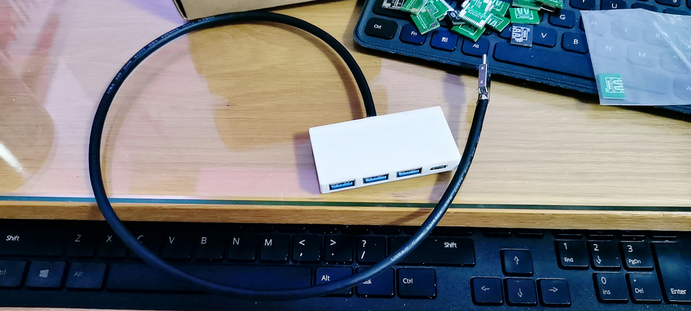
USB 3.0 expansion dock adapter board
A project with a troubled fate
Last October, LCSC released a tutorial on designing a four-layer board for a USB 3.0 docking station,

which looked quite appealing. I thought I'd get one too, so I started browsing Taobao to buy components. Then I found a super cheap VL813 board:

I immediately ordered 5 RMB worth, since even just disassembling the chip would be profitable!
After the board arrived, I thought about saving costs and decided to go all the way. So I designed a USB-C female connector adapter board, soldered it to the original soldering positions, and
ordered it again. After soldering and connecting it to the computer... damn, it only recognized USB 2.0.

I suspected an impedance mismatch issue, so I modified it to a four-layer board and redesigned it, but it still didn't work...

In the end, I bought a USB 3.0 cable and a Type-C male connector, soldered them according to the original design, and used it
for about half a year. One day, while browsing the open-source forum, I saw an open-source portable SSD on the homepage. One sentence in the description caught my attention:

since changing the female connector to a male connector requires swapping, does the reverse also apply?
I immediately redesigned and tested it, and sure enough, it worked!


However, it wasn't completely finished; one board still wouldn't power on...
Following the 5V lead, I discovered a power failure on a DC-DC chip.

The VIN pin was receiving 5V, but there was no output. Based on my experience with Cat Wireless, I should measure the chip's enable signal. Sure enough, the EN pin only had 0.2V. To be safe, I compared it with a working board. The working board's EN pin normally has around 2.3V, so it was basically confirmed to be an enable signal problem.
Continuing to investigate, I found that the EN pin's enable signal was derived from the 5V on the back of the board, passing through vias and then through several 0402 resistors for voltage division. I could measure 5V at the capacitor on the back of the board, but only 0.3V on the front. A broken trace was immediately detected. I took out a polishing pen, smoothed out the pads, and added jumper wires.

That solved the problem with the USB port; it was also a broken trace on a power pin, so I added a thicker jumper wire.
Finally, I drew a nice-looking casing and declared the tinkering over!


PDF_USB3.0 Expansion Dock Adapter Board.zip
Altium_USB3.0 Expansion Dock Adapter Board.zip
PADS_USB3.0 Expansion Dock Adapter Board.zip
BOM_USB3.0 Expansion Dock Adapter Board.xlsx
95235
electronic


 京公网安备 11010802033920号

 PAL16H8CSGSTD


