In what area does the varactor diode work normally? What is the working principle of the varactor diode?
Source: InternetPublisher:sigma Keywords: Diode Varactor Updated: 2025/03/07
In what area does the varactor diode work normally?
Reverse voltage bias region.
The external conditions for the operation of the varactor diode are similar to those of the Zener diode. It must operate in the reverse voltage bias region (the Zener diode operates in the reverse breakdown state). When a reverse voltage is applied to both ends of the varactor diode, the PN junction inside it becomes thicker. The higher the reverse voltage, the thicker the PN junction. Since the PN junction prevents current from passing through, the varactor diode is in the cut-off state when it is working. Here, the PN junction is equivalent to the insulating medium between the two plates of an ordinary capacitor.
The P-type semiconductor and N-type semiconductor are equivalent to the two plates of an ordinary capacitor, that is, the varactor diode in the cut-off state will form a structure equivalent to a parallel plate capacitor inside, and this "capacitor" is called junction capacitance. The P-type semiconductor and N-type semiconductor of an ordinary diode are relatively small, and the junction capacitance formed is very small and can be ignored; while the varactor diode is manufactured by deliberately increasing the area of the P-type semiconductor and the N-type semiconductor, thereby increasing the junction capacitance, greatly enhancing the capacity and variable capacitance effect under reverse bias conditions.
The size of the junction capacitance of the varactor diode is related to the size of the reverse voltage. The higher the reverse voltage, the smaller the junction capacitance; the lower the reverse voltage, the larger the junction capacitance. The relationship curve between the junction capacitance and the reverse voltage intuitively shows the change law of the reverse voltage and the junction capacitance at both ends of the varactor diode. The relationship between the junction capacitance and the reverse voltage is nonlinear. In order to overcome the nonlinearity, correction networks, high bias voltages, and multiple loops can be used in actual use.
Working Principle of Varactor Diode
To understand how a varactor works, you first need to understand how a variable capacitor works:
A capacitor consists of two conductive surfaces separated by a non-conductive dielectric (see figure below). When one surface is connected to a positive voltage and the other to a negative voltage, positive charge accumulates on one surface and negative charge accumulates on the other surface due to the attraction between positive and negative charge carriers.
The amount of charge that accumulates is called capacitance. If we reduce the gap between the two surfaces, the attraction between the positive and negative charge carriers increases, so more charge accumulates on the surfaces, i.e. the capacitance increases.
The opposite happens when the surfaces move away from each other, i.e. the capacitance decreases. A variable capacitor has a mechanical arrangement that allows us to vary the gap between the surfaces, effectively varying the capacitance.

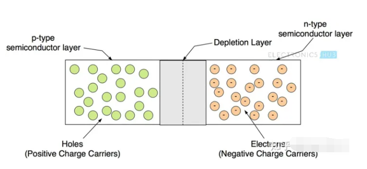
Now let's go back to the working principle of the pn junction diode. The p-type layer of the diode is filled with positive charge carriers and the n-type layer is filled with negative charge carriers. Near the contact surface between the two layers, the positive and negative charges diffuse and neutralize each other. This region is called the depletion region.
Unless an external voltage is applied, it is not possible for the charge carriers to diffuse further through the depletion layer. Hence, the depletion layer effectively acts as an insulator.
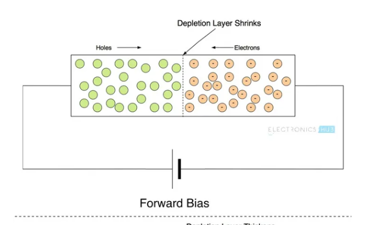
The width of the depletion layer depends on the voltage applied to the p- and n-type layers. If a forward bias is applied, i.e. a positive voltage is applied to the p-type layer and a negative voltage is applied to the n-type layer, the width of the depletion region decreases, and above a certain voltage it disappears completely.
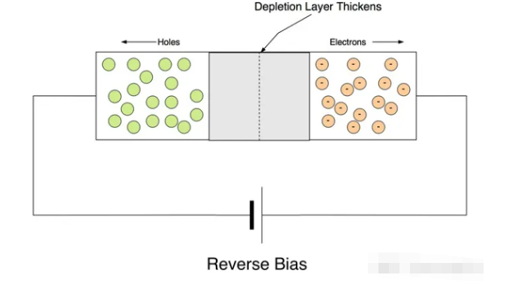
If a reverse bias is applied, that is, a positive voltage is applied to the n-type layer and a negative voltage is applied to the p-type layer, the width of the depletion layer increases. The following figure illustrates these two situations:
In simple words, the width of the depletion region can be changed to the desired value simply by adjusting the voltage across the p&n type semiconductor layer. So, by now, you must have observed the similarities between a capacitor and a reverse biased diode. The depletion layer in a diode is similar to the dielectric in a capacitor, which acts as an insulator and prevents the charge carriers from flowing from one side to the other.
Therefore, when a reverse bias is applied across the diode, the corresponding charge carriers accumulate on either side of the depletion layer. This causes the diode to gain some capacitance, known as the junction capacitance.
Varactor diodes are specifically designed to enhance this ability to store charge carriers when a reverse bias is applied, causing them to act as a capacitor.
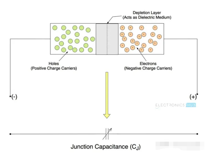
The junction capacitance is inversely proportional to the width of the depletion layer, i.e., the smaller the width of the depletion layer, the higher the capacitance and vice versa. Therefore, if we need to increase the capacitance of the varactor, the reverse bias voltage should be reduced. It causes the width of the depletion layer to decrease, resulting in higher capacitance. Similarly increasing the reverse bias voltage should reduce the capacitance.
This ability to achieve different capacitance values simply by varying the applied voltage is the greatest advantage of the varactor diode compared to ordinary variable capacitors.
Application fields of varactor diodes
Varactor diodes are widely used in radio, communications, control systems and other fields, including:
Frequency synthesizer: used to generate precise frequency signals.
Controlled oscillator: used to generate a stable high-frequency oscillation signal.
Power transformer: used to regulate high frequency current.
- Diode voltage regulator circuit sharing
- Characteristics, advantages and disadvantages of CISC architecture
- LM337 pin diagram and parameters, LM337 application circuit diagram
- What is a photocoupler and how to select and use one?
- What is a FinFET? What are the advantages and disadvantages of FinFET?
- What is the difference between single-phase and three-phase power? When is three-phase power required?
- An article explains the working principle of the Wheatstone bridge
- How does a series arrangement of Zener diodes affect the electrical behavior?
- What is the relationship between capacitance and impedance in an AC circuit? How do you calculate the impedance of a capacitor?
- How do you calculate the value of capacitors in series? Why use capacitors in series?
- SKiiPPACK unit circuit
- Analysis of various power supply filter circuits
- Acousto-optic digital level detector circuit diagram
- 3 and 1/2 digit digital thermometer using diode as temperature sensor
- High frequency signal input switch circuit b
- Tuning circuit composed of TA7335P
- Mixing circuit
- Indicator circuit with series connected diodes
- PLC input and output wiring a
- Diode spark suppression circuit a


 京公网安备 11010802033920号