How to enhance power and signal integrity through low noise?
Source: InternetPublisher:念慈菴 Keywords: Power Signal Integrity Low Noise Updated: 2025/02/25
When engineers design power supplies for noise-sensitive systems in medical applications, test and measurement, and wireless infrastructure that use clocks, data converters, or amplifiers, one common problem they face is how to improve accuracy and precision while minimizing system noise. Since different people understand the term "noise" differently, I would like to clarify that the noise discussed in this article refers to the low-frequency thermal noise generated by resistors and transistors in the circuit. You can usually think of the noise in the 10Hz to 100kHz bandwidth of the noise spectral density curve (in microvolts per square root hertz) as the integrated output noise (in rms millivolts). Power supply noise can degrade the performance of analog-to-digital converters and cause clock jitter.
In the past, clocks, data converters, or amplifiers were powered by a DC/DC converter (or module), a low dropout regulator (LDO) (such as the TPS7A94, TPS7A82, TPS7A84, TPS7A52, TPS7A53, or TPS7A54), and a ferrite bead filter arrangement, as shown in Figure 1. This design approach minimizes power supply noise and ripple and maintains good performance when the load current is less than about 2A. However, as the load increases, power losses in the LDO cause efficiency and thermal management issues. For example, a post-regulator LDO can add 1.5W of power loss in a typical analog front-end application. Is a low-noise, high-efficiency design impossible? Not necessarily.
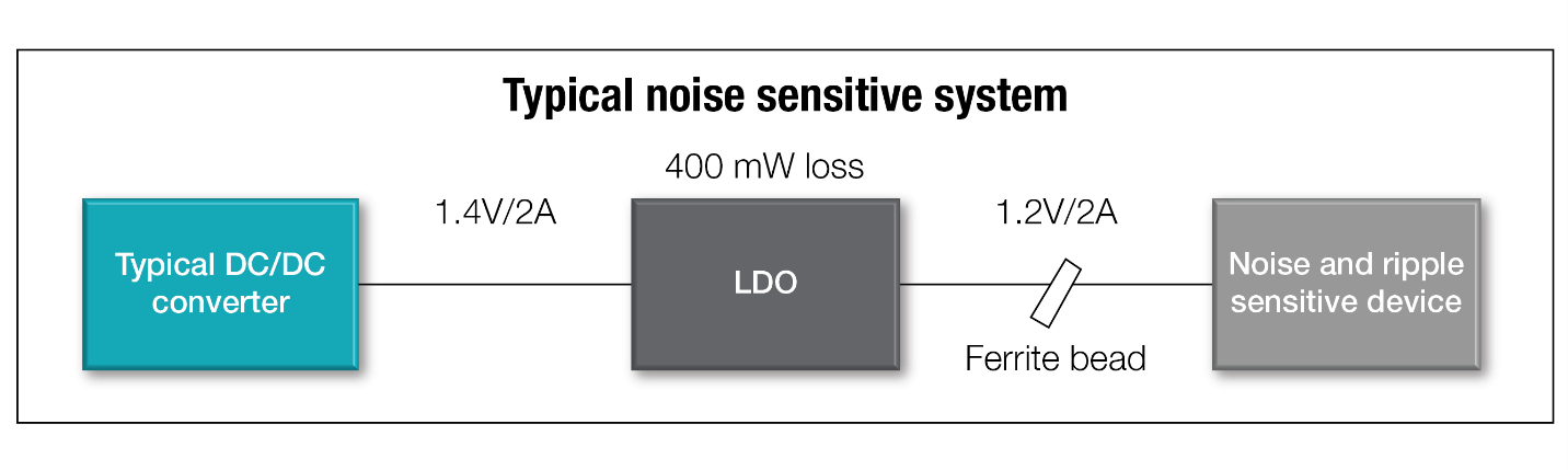
Figure 1: Typical low-noise architecture using a DC/DC converter, LDO, and ferrite bead filter
One way to prevent power loss is to minimize the voltage drop across the LDO. However, this approach can negatively impact noise performance. In addition, higher current LDOs are typically larger, which increases design size and cost. A more effective way to ensure low noise without increasing power loss is to replace the LDO in the design with a low noise DC/DC buck converter or module, as shown in Figure 2.
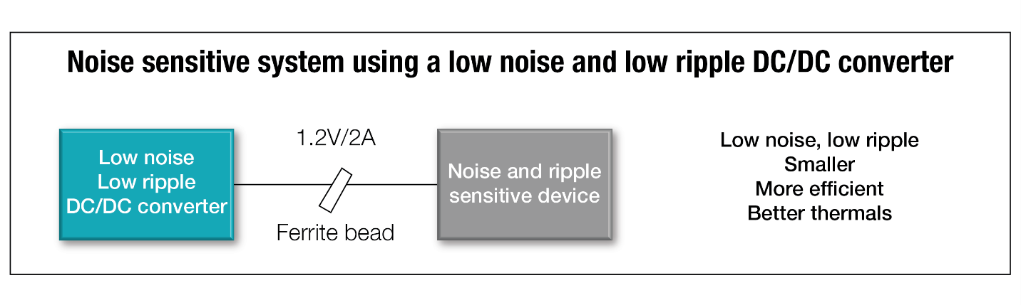
Figure 2: Using a low-noise buck converter (no LDO)
I know what you are asking: How can you still provide a low noise power supply by removing the main device for noise reduction? Well, many LDOs have a low pass filter at the bandgap reference to minimize the noise that enters the error amplifier. The TPS62912 and TPS62913 families of low noise step-down converters and the TPSM82912 and TPSM82913 modules use a capacitor connected to the noise reduction/soft start pin and form a low pass resistor/capacitor filter with the integrated Rf and externally connected CNR/SS as shown in Figure 3. Essentially, this structure emulates the performance of a bandgap low pass filter in an LDO. If the TPS62913 or TPSM82913 still does not meet your low noise requirements, you can use a low noise LDO with lower dropout and power consumption (such as the TPS7A94) that still achieves ultra low noise. Application brief SBVA099 explains this in more detail.
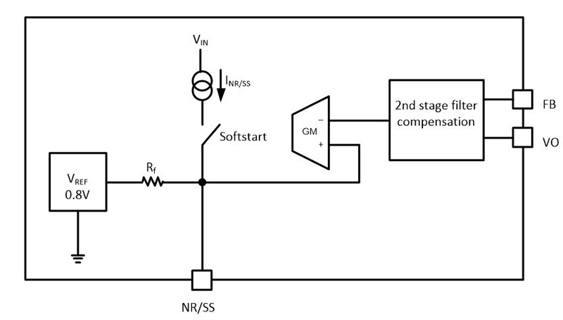
Figure 3: Low-noise buck block diagram with bandgap noise filtering
How to reduce output voltage ripple? All DC/DC converters generate output voltage ripple at their switching frequency. In precision systems, noise-sensitive analog power rails require ultra-low supply voltage ripple to minimize frequency spurs in the spectrum. Supply voltage ripple is usually determined by the DC/DC converter's switching frequency, inductor value, output capacitance, equivalent series resistance, and equivalent series inductance. To reduce the ripple generated by these components, engineers often use LDOs and/or small ferrite beads and capacitors to form a π-type filter to minimize load ripple. Low-ripple buck converters such as the TPS62912 and TPS62913, as well as the TPSM82913 module, take advantage of ferrite bead filters by integrating ferrite bead compensation and remote sensing feedback. By utilizing the inductance of the ferrite bead and the additional output capacitor, the high-frequency component in the output voltage ripple is eliminated and the ripple is reduced by about 30dB, as shown in Figure 4.
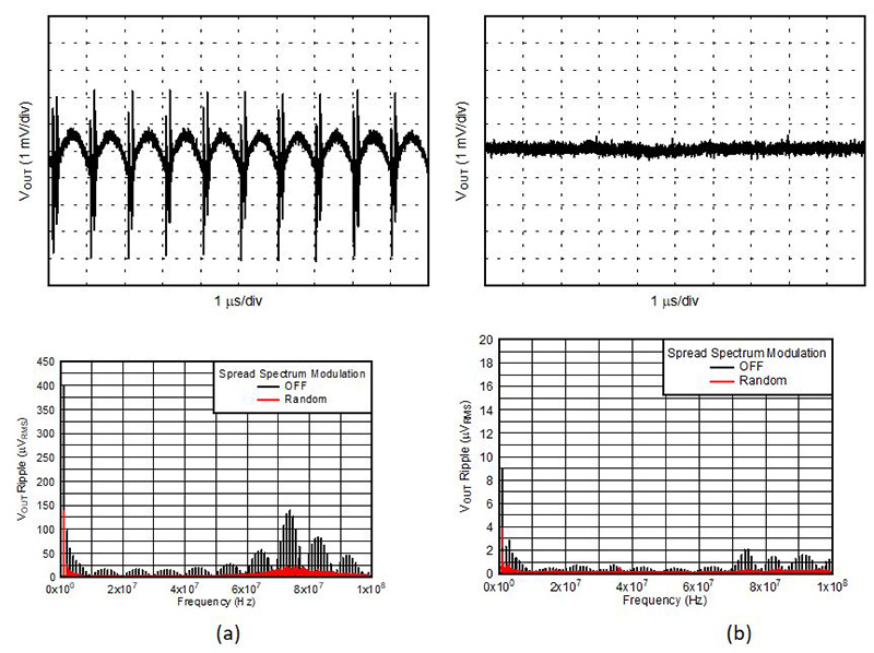
Figure 4: Output voltage ripple before using a ferrite bead filter (a); output voltage ripple after using a ferrite bead filter (b)
in conclusion
By integrating features that reduce system noise and ripple, low-noise buck converters help engineers achieve low-noise power solutions without LDOs. Of course, different applications require different noise levels, and different output voltages require different performance. So, you can only choose the right low-noise architecture for your design. If you want to simplify noise-sensitive analog power design, reduce power losses, and reduce overall design size, consider using a low-noise buck converter.
- How does a step-down switching regulator use a series transistor or a power MOSFET?
- What effect does the copper coating on the bottom of the inductor have on the power supply?
- How to ensure the stable performance of SSD when the voltage is unstable?
- How much current can a 2N3055 solar cell produce? How can I get 3055V from a 12N2 solar cell?
- In-depth analysis of DC-AC converter inverter
- Visible laser digital control modulation driver
- Driving circuit that controls LED brightness using PWM signal
- Current/voltage conversion circuit using current converter
- UC3842 Electric Vehicle Charger
- MIC4680 constant current charger
- Insulation Basics: Choosing the Right Insulation Solution for Your Application
- Provides USB Type-C® port chip solutions for lithium battery-powered devices
- Is the power module usually called a power supply?
- How should the inductor of the switching power supply be placed correctly in PCB design?
- What determines the input power of a power supply?
- Design and development trends of power modules
- The reason why the power supply should be set to +3.3V
- Low noise preamplifier (b)
- High-speed preamplifier for measurement that reduces noise with dual transistors
- Low noise instrument amplification circuit diagram


 京公网安备 11010802033920号