Sharing layout and tips for multi-rail power supply design
Source: InternetPublisher:偷熊计划 Keywords: Power supply design power rail Updated: 2025/02/11
In this article, various details of power budget and board layout will be highlighted. Since many application boards require multiple power rails, this series examines multi-power board solutions. The goal is to achieve a high-quality initial design through good component placement and routing to highlight some power budget and routing tips and tricks.
Power supply design can be divided into three main stages: (1) design strategy and IC selection; (2) schematic design, simulation and testing; (3) layout and routing. Investing time in the (1) design and (2) simulation stages can prove the validity of the design concept, but the real test requires putting it all together and testing it on a desktop. In this article, we will focus on how to wire it.
In power supply design, careful layout and routing are critical to a robust design with adequate margins in size, accuracy, efficiency, and avoiding production problems. Years of bench experience help, so rely on the knowledge of the layout engineer for the final finish of board fabrication.
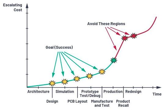
A design may look solid on paper (i.e. from a schematic perspective) and may even simulate without problems, but the real test comes after layout, PCB fabrication, and prototype stress testing by loading the circuit. This section highlights some tips and tricks to avoid pitfalls by using real-world design examples. Some important concepts help avoid design flaws and other pitfalls that may lead to a redesign and/or PCB respin. Figure 1 shows how costs can quickly escalate if a design enters production without careful testing and margin analysis.
Power Budget
Watch for systems that operate as expected under normal conditions, but not in full-speed mode or when they begin to exhibit erratic data (when noise and interference are excluded).
Avoid current limiting situations when tapping cascade stages. Figure 2 shows a typical cascade application: The figure shows a design consisting of an ADP5304 buck regulator (PSU1) that generates a 3.3V supply with a maximum current of 500mA. To improve efficiency, designers should tap the 3.3V rail instead of the input 5V supply. The 3.3V output is further tapped to power PSU2 (LT1965), which is an LDO regulator used to further regulate to 2.5V with a maximum output current of 1.1A, which meets the requirements of the on-board 2.5V circuits and ICs.
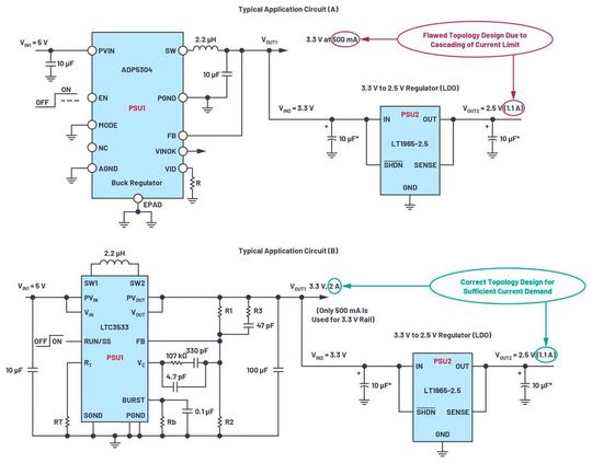
This is a system with some classic hidden problems. The system works fine under normal conditions. But problems arise when the system initializes and starts running at full speed - for example, when a microprocessor and/or ADC starts sampling at high speed. Since no regulator can produce more power at its output than at its input, the maximum power at VOUT1 (P = V × I) in Figure 2a is 3.3V × 0.5A = 1.65W to be delivered to the combined circuit of VOUT1 and VOUT12. This assumes 100% efficiency, so less power is available due to power supply losses. Assume that the maximum available power for the 2.5V rail is 2.75W. If the circuits try to demand this much power, they will not be met, resulting in erratic behavior when PSU1 starts to reach current limit. Current may start to limit due to PSU1, or worse, some regulators will shut down completely due to overcurrent.
If Figure 2a is implemented after successful troubleshooting, a higher power regulator may need to be replaced. The best case is a pin-compatible higher current replacement; the worst case is a complete redesign and re-spin of the PCB. By keeping the power budget in mind before the design concept phase, potential project timeline delays can be avoided (see Figure 1).
With this in mind, before selecting one or more regulators, create a realistic power budget. Include all required power rails: 2.5V, 3.3V, 5V, etc. Include all pull-up resistors, discrete devices, and ICs that consume power for each rail. Use these values and reverse-calculate your power requirements, as shown in Figure 2b. Using the Power Tree System Design Tool, it is easy to create a power tree that supports the required power budget.
Placement, Tracking, and Routing
Proper layout, routing, and routing can avoid current capacity limitations due to burned traces caused by wrong trace width, wrong vias, insufficient number of pins (connectors), wrong contact size, etc. The following section includes some PCB design tips worth noting.
Connectors and Pin Headers
Expanding the example shown in Figure 2 to a total current of 17A, the designer must consider the current handling contact capability at the pin (or pins), as shown in Figure 3. In general, the current carrying capacity of a pin or contact depends on several factors, such as the physical pin size (contact area), metal composition, etc. A typical through-hole male header pin with a diameter of 1.1mm1 is about 3A. If 17A is required, make sure your design has enough current pins to handle the total current carrying capacity. This is easily accomplished by multiplying the current carrying capacity of each conductor (or contact) and some safety margin over the total current draw of the PCB circuit.

In this example, to reach 17A you need 6 pins (with 1A headroom). VCC and GND require a total of 12 pins. To reduce the number of contacts, consider using a power jack or larger contacts.
Routing
Use available online PCB tools to help determine current capabilities in your layout. A 1oz copper PCB with a 1.27mm trace width yields approximately 3A of current carrying capability, while a 3mm trace width yields approximately 5A of current carrying capability. Leaving some headroom, a 20A track requires a width of 19mm (approximately 20mm) (note that temperature rise is not considered in this example). As can be seen in Figure 3, a 20mm track width is not feasible due to space constraints for the PSU and system circuitry. To address this, a simple solution is to use multiple PCB layers. Reduce the trace width (for example, to 3mm) and duplicate those traces to all available layers in the PCB to ensure that the total combined traces (in all layers) meet at least the 20A current capability.
Vias and splicing
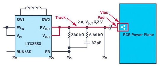
Figure 4 shows an example of vias stitching a PCB power plane from a voltage regulator. If a 1A via is selected and your power requirement is 2A, the track width must be able to carry 2A and the via stitching must also be able to handle it. The example in Figure 4 requires at least two vias (preferably three if space is available) to stitch the current to the power plane. This is often overlooked when only a single via is used for stitching. When completed, the via acts like a fuse that blows and disconnects power to adjacent planes. An under-designed via can be difficult to troubleshoot because the via may not be obvious or it may be difficult to see if it is blocked by a component.
Note the following parameters for vias and PCB traces: Trace width, via size, and electrical parameters depend on several factors that affect the final current-carrying capacity, such as PCB plating, routing layers, operating temperature, etc. Previous PCB design tips do not take these dependencies into account, but designers should be aware of them when determining layout parameters. Many PCB trace/via calculators are available online. It is highly recommended that designers consult their PCB manufacturer or layout engineer after the schematic design and keep these details in mind.
Avoid overheating
Many factors can cause heat dissipation issues, such as the housing, airflow, etc., but this section focuses on the exposed pad. If properly connected to the board, a regulator with an exposed pad has a lower thermal resistance. Generally speaking, if the regulator IC has a power MOSFET designed into the chip (i.e. it is monolithic), then the IC usually has an exposed pad for heat dissipation. If the converter IC uses an external power MOSFET (it is a controller IC), then the control IC usually does not need an exposed pad because the main heat source (the power MOSFET) is external to the IC.
Typically, these exposed pads must be soldered to the PCB ground plane to be effective. There are exceptions depending on the IC, as some specify that they can be connected to an isolated soldered PCB area to act as a heatsink for a heat sink. If unsure, refer to the datasheet for the part in question.
When you connect an exposed pad to a PCB plane or isolated area, make sure to connect these vias (many of them in array form) to the ground plane for heat dissipation (heat transfer). For multi-layer PCB ground planes, it is recommended to connect the required ground planes under the pad (on all layers) with vias.
- Basic characteristics of power field effect tubes, how to improve the dynamic performance of power MOSFET
- A very convenient small power supply circuit to share
- Fabrication of multi-cell lithium battery charging circuit
- Driving circuit of switching power supply field effect tube
- Transformerless AC-DC constant current LED driver circuit
- Parallel DC regulated power supply circuit diagram
- Boost drive circuit composed of RT8450
- An ultra-low output voltage regulator
- Power supply circuit that can reduce LM317 ripple
- The production of adjustable voltage-stabilized power supply composed of LM317
- 24V power supply pure flat display high voltage power supply circuit diagram
- Solar power circuit
- audio power circuit
- Additional power circuit design for USB devices
- Household emergency power circuit
- Common power circuits and applications 09
- Common power circuits and applications 08
- 5V uninterruptible power supply circuit
- ±5V, ±12V power circuit A
- CASPER TM-5158 VGA color display power supply circuit


 京公网安备 11010802033920号