Working principle and truth table of JK flip-flop
Source: InternetPublisher:newlandmark Keywords: Truth table flip-flop Updated: 2025/01/10
The JK flip-flop is a flip-flop that can be set, reset, and toggled. It can be used to make counters, event detectors, frequency dividers, and more.
In this tutorial, you will learn how it works, its truth table, and how to build one using logic gates.
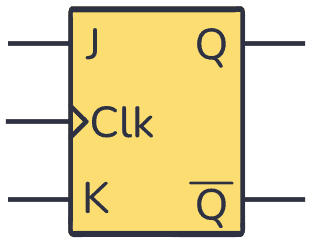 JK flip-flop symbol
What is a JK flip-flop?
Flip-flops are components that can store digital values on their outputs. They have a clock input (Clk) that determines when the output state can be changed.
Contrary to what you might think, JK
The two inputs of the Flip-Flop, "J" and "K", are not abbreviations of the pins' functions (as is the case with the SR latch). Their inventor, Jack Kilby (JK), chose them to distinguish his flip-flop design from other types of flip-flops.
You can see a basic implementation of this circuit below. It is based on an SR latch, built with NAND gates:
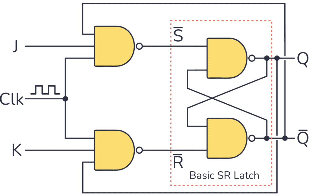 JK flip-flop basic circuit
The J and K inputs of a JK flip-flop can be used to set, reset, or toggle the output as follows:
J=1 and K=0 sets the output to 1
J=0 and K=1 reset the output to 0
J=1 and K=1 switch output
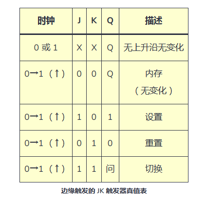
But for a flip-flop to make any changes, its clock input must be 1. Look at the truth table below:
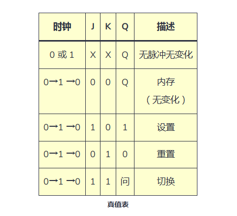
Clock JKQ Description
0XXQClk in 0 Q None
change
100Q Memory
(No change)
1101 Settings
1010 Reset
111 Questions Switch
JK Flip-Flop Truth Table
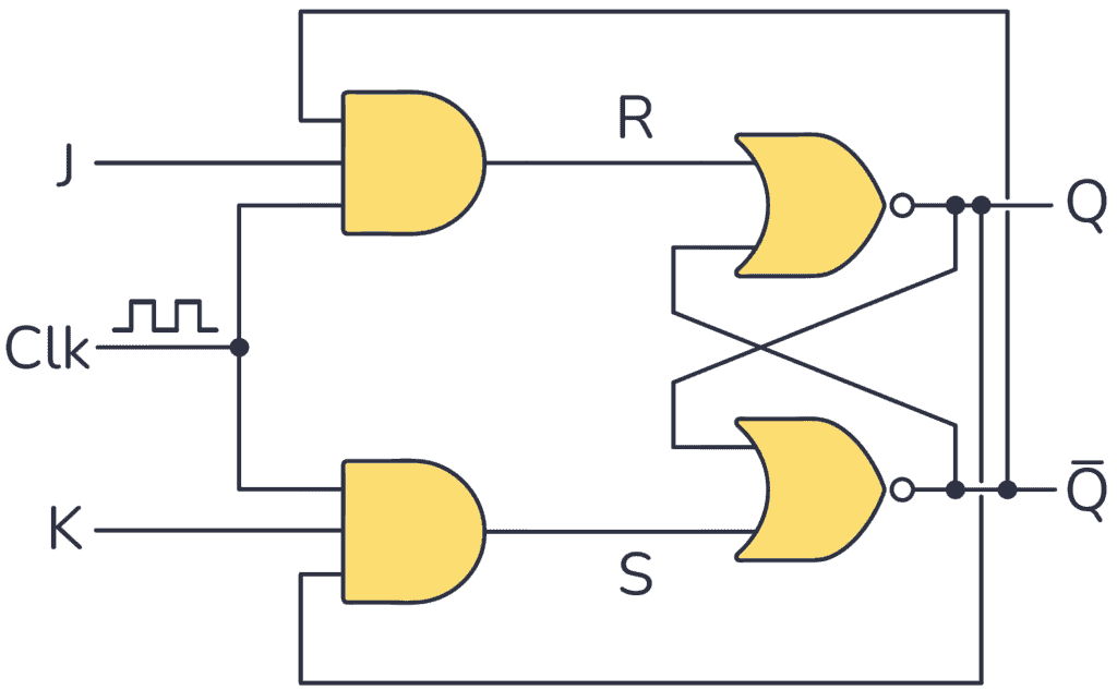
Another way to implement the basic JK flip-flop circuit is to use two AND gates and two NOR gates as shown below (it works exactly the same as if built using NAND gates):
Racing Problems
In principle, the basic implementation above works, but there will be timing problems. When the clock is at "1" and you want to toggle the output, it will toggle between "1" and "0" very quickly until the clock goes back to "0". This problem is called a race condition.
You can fix this by making the trigger pulse triggered or edge triggered.
Pulse triggered JK flip-flop
Below is a pulse-triggered JK flip-flop based on the master-slave principle:
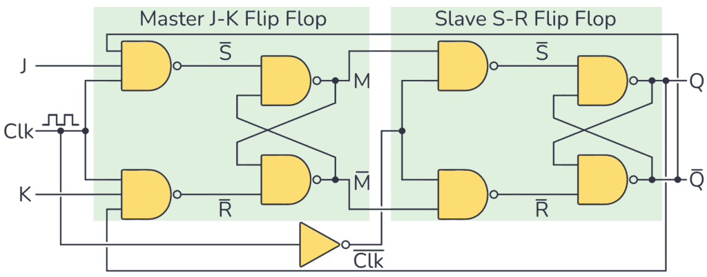 Master-slave circuit
As you can see, to build this configuration you need a basic JK flip-flop circuit connected together with an SR flip-flop.
To understand how this version works, take a look at the timing diagram below:
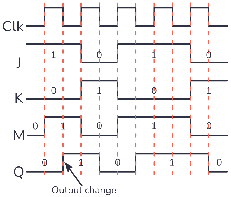
Once the clock generates a rising edge↑, that is, from 0 to 1 (0→1
), it triggers the master part. As a result, the value of the output in this part changes. These signals are connected to the slave part, but this does not trigger on the rising edge because the clock is already inverted.
Once the clock signal generates a falling edge↓, changing from 1 to 0 (1→0), it triggers the slave part, causing the Q output to reflect the output value of the master.
Therefore, this circuit requires a complete pulse (0 → 1 → 0) to change the output. This is why this configuration is called a pulse-triggered JK flip-flop.
Edge-triggered JK flip-flop
Unlike master-slave designs that require a complete pulse, you can also build edge-triggered designs that trigger from a rising edge↑ or a falling edge↓.
The following is the timing diagram for rising edge triggering:

The diagram above shows how this circuit only requires a rising edge on the Clk input to change the state of output Q. It will only change on rising edges.
To build a JK flip-flop that is triggered only by rising-edge signals, you can use a rising-edge-triggered D flip-flop, a NOT gate, and a NAND gate as follows:
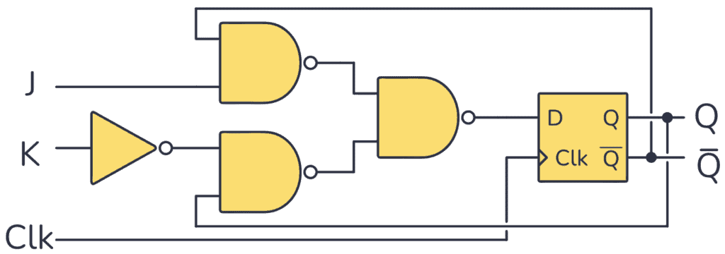
Edge-triggered JK flip-flop circuit
- Which one is better, NPN or PNP transistor?
- The Importance and Ideal Model of Impedance Matching
- What are the main types of resistors? Detailed explanation of the functions and uses of resistors
- Types and structures/characteristics/functions/implementations of smart sensors
- How does sand become chips?
- Advantages and disadvantages of organic semiconductors, the conductive mechanism of organic semiconductors
- What are the parts of the fpga design process
- What is a D flip-flop and how does it work?
- DIY a decorative lamp
- Experimental circuit based on 4040 binary adder counter
- CC4528 dual monostable flip-flop design multivibrator circuit diagram
- Frequency divider circuit with adjustable frequency division ratio
- Counter composed of 4 T flip-flops
- Bad books do not bind circuits
- Flip-flop timing circuit composed of photodiodes, etc.
- Thyristor circuit diagram of integrated flip-flop td1028
- Gantry milling machine trigger schematic circuit
- electronic flash trigger.gif
- Frequency divider composed of flip-flops
- high speed trigger


 京公网安备 11010802033920号