The Importance and Ideal Model of Impedance Matching
Source: InternetPublisher:刘德华河北分华 Keywords: Impedance matching load impedance excitation source Updated: 2025/01/21
1. What is impedance matching?
I believe everyone has learned in circuit principles that when the load resistance of a circuit is large, its output power is maximum;
Impedance matching refers to a working state in which the load impedance and the internal impedance of the excitation source are adapted to each other to obtain the maximum power output. For circuits with different characteristics, the matching conditions are different.
In a purely resistive circuit, when the load resistance is equal to the internal resistance of the excitation source, the output power is maximum. This working state is called matching, otherwise it is called mismatch.
Impedance control is a relatively important link in hardware design. IC manufacturers generally provide terminal manufacturers with some relevant reference design suggestions such as PCB board material, PCB stacking, PCB board thickness, etc. for their applications (these are all closely related to PCB impedance control design). After obtaining these materials, terminal manufacturers will make localized design adjustments based on actual conditions, and then provide relevant design information and requirements to PCB manufacturers for PCB production.
There are different characteristic impedance values for different signal systems, such as 75ohm, 100ohm, 90ohm, 50ohm, etc. For higher frequency RF signals, the most common impedance control is 50ohm.
2. The Importance of Impedance Matching
Impedance matching refers to achieving a suitable match between the signal source or transmission line and the load. Impedance matching has two main functions: adjusting load power and suppressing signal reflection.
In actual PCB design, RF transmission lines usually use microstrip and stripline routing, and reference layers need to be selected for impedance control. Considering the RF characteristics of the chip, the actual PCB production process, and the materials used for components, in addition to the impedance control of the PCB RF transmission line, some matching network circuits usually need to be added in the hardware design for RF debugging.
The role of impedance matching mainly has the following aspects
1. Adjust the load power
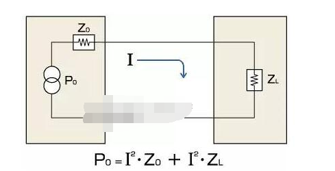
As shown in the figure below: Assuming that the excitation source is fixed, the power of the load is determined by the impedance matching of the two. For an idealized pure resistance circuit or low-frequency circuit, the reactance value caused by inductance and capacitance can be basically ignored. At this time, the impedance source of the circuit is mainly resistance. As shown in Figure 2, the current in the circuit is I=U/(r+R), and the load power P=I*I*R. From the above two equations, it can be obtained that when R=r, P reaches the maximum value, Pmax=U*U/(4*r).

2. Suppress signal reflection
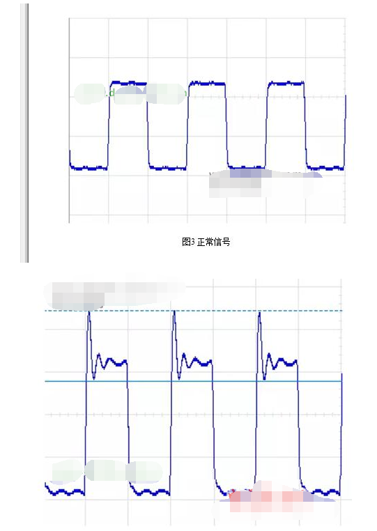
When a beam of light is emitted from air to water, reflection occurs because the optical conductivity of light and water is different. Similarly, reflection will also occur if a characteristic impedance mutation occurs on the transmission line during signal transmission. The wavelength is inversely proportional to the frequency. The wavelength of a low-frequency signal is much longer than the length of the transmission line, so reflection is generally not a problem. In the high-frequency field, when the wavelength of the signal is of the same order of magnitude as the length of the transmission line, the reflected signal is easily mixed with the original signal, affecting the signal quality. Impedance matching can effectively reduce and eliminate high-frequency signal reflections.
3. Adjustment of resonant frequency and bandwidth
4. Debugging of indicators such as power, EVM, ACLR, PA current, conducted spurious and radiated spurious, etc.
3. Ideal model of impedance matching
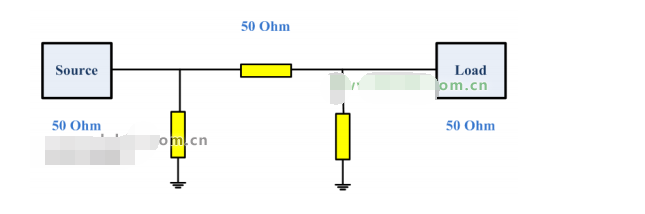
Most RF engineers have encountered the problem of impedance matching. Generally speaking, the purpose of impedance matching is to ensure the effective transmission of signals or energy from the "signal source" to the "load". The most ideal model is of course to hope that the output impedance of the Source end is 50 ohms, the impedance of the transmission line is 50 ohms, and the input impedance of the Load end is also 50 ohms. 50 ohms all the way down is the most ideal.
Impedance matching to the ideal model
However, the actual situation is: the source impedance will not be 50ohm, and the load impedance will not be 50ohm. At this time, several impedance matching circuits are needed, and the matching circuit is composed of inductors and capacitors. At this time, we need to use capacitors and inductors to debug the impedance matching circuit to achieve optimal RF performance.
In a common broadband amplifier, since the output impedance is 50Ω, impedance matching needs to be considered in the power transmission circuit. However, in reality, when the length of the cable is negligible for the wavelength of the signal, impedance matching is not necessary.
Considering that the signal frequency is 1MHz, its wavelength is 300m in air and about 200m in coaxial cable. In the commonly used coaxial cable with a length of about 1m, it is within the completely negligible range. (Figure H)

If there is impedance, power will be consumed in the impedance, so failure to match the impedance will result in useless waste of the amplifier's output power.
4. Impedance matching method
There are two main methods of impedance matching: one is to change the group impedance, and the other is to adjust the transmission line.
Changing the impedance means adjusting the load impedance value by connecting capacitors, inductors and loads in series or parallel to achieve source and load impedance matching.
Adjusting the transmission line is to lengthen the distance between the source and the load, and adjust the impedance to zero with the capacitor and inductor. At this time, the signal will not be transmitted, and the energy can be absorbed by the load. In high-speed PCB wiring, the routing impedance of digital signals is generally designed to be 50 ohms. It is generally stipulated that the baseband of coaxial cable is 50 ohms, the frequency band is 75 ohms, and the twisted pair (differential) is 85-100 ohms.
- What is an ac to dc transformer in circuit design
- How do Zener diodes protect circuits?
- In-depth analysis of energy losses in oscillation frequencies
- What are the parts of the fpga design process
- How do you calculate the value of capacitors in series? Why use capacitors in series?
- Working principle and truth table of JK flip-flop
- Working principle/characteristics/application fields/equivalent circuit of unijunction transistor
- DIY a decorative lamp
- What is the difference between JFET and MOSFET
- Common electrical circuits: frequency-selective (bandpass) amplifier circuit
- High frequency impedance matching amplifier
- 555 square wave oscillation circuit
- 555 photo exposure timer circuit diagram
- Introducing the CD4013 washing machine timer circuit diagram
- Simple level conversion circuit diagram
- 555 electronic guide speaker circuit diagram for blind people
- Circuit diagram of disconnection alarm composed of 555
- Analog circuit corrector circuit diagram
- color discrimination circuit
- Color sensor amplification circuit


 京公网安备 11010802033920号