Transfer characteristics of BJT, how to apply Shockley equation?
Source: InternetPublisher:睡不醒的小壮 Keywords: BJT Bipolar Transistor Updated: 2025/01/10
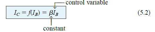
In a BJT or bipolar transistor, the transfer characteristic can be understood as a graph of the output current versus the input control amplitude, thus showing a direct "transfer" of the variable from input to output in the curve represented in the graph.
We know that for a bipolar junction transistor (BJT), the output collector current IC and the control input base current IB are related by a parameter β, which is assumed to be a constant in the analysis.
Referring to the equation below, we see that there is a linear relationship between IC and IB. If we double the IB level, the IC will also double proportionally.
Unfortunately, this convenient linear relationship may not be true for the input and output amplitudes of a JFET. Instead, the relationship between drain current ID and gate voltage VGS is defined by the Shockley equation:
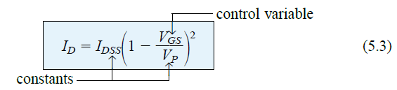
Here, the squared expression is responsible for the nonlinear response on ID and VGS, with the curve increasing exponentially as the magnitude of VGS decreases.
Although for DC analysis the mathematical approach is easier to implement, a graphical approach may require plotting the above equations.
This can present a plot of the device in question as well as the network equations relating to the same variables.
We find the solution by looking at the intersection of the two curves.
Keep in mind that when you use the graphical approach, the characteristics of the device are not affected by the network that implements the device.
As the intersection point between the two curves changes, it also changes the network equation, but this has no effect on the transfer curve defined in equation 5.3 above.
So, in general we can say:
The transfer characteristics defined by the Shockley equations are not affected by the network in which the device is implemented.
We can obtain the transfer curve using the Shockley equation or from the output characteristic depicted in Figure 5.10
In the image below we can see two graphs. The vertical line measures milliamps for both graphs.
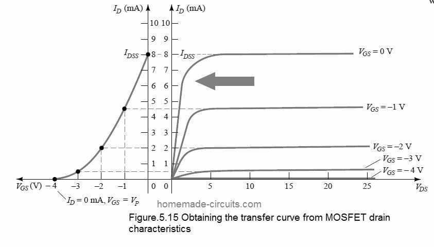
One graph plots the drain current ID versus the drain-source voltage VDS and the second graph plots the drain current versus the gate-source voltage or ID versus VGS.
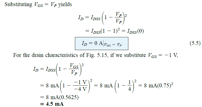
With the drain characteristics shown on the right side of the “y” axis, we are able to draw a horizontal line starting from the saturation region of the curve, shown as VGS = 0 V, to the axis shown as ID.
Therefore, the current level reached by both graphs is IDSS.
The intersection point on the ID vs. VGS curve is shown below, since the vertical axis is defined as VGS = 0 V

Note that the drain characteristic shows the magnitude of one drain output versus another, with both axes explained by variables in the same region of the MOSFET characteristic.
Therefore, the transfer characteristic can be defined as a plot of the MOSFET drain current versus the quantity or signal that is the input control.
Therefore, when the curve is used on the left side of Figure 5.15, this results in a direct "shift" across the input/output variables. If it were a linear relationship, the plot of ID vs VGS would be across IDSS and VP
straight line.
However, this results in a parabolic curve because VGS spans the vertical spacing between the drain features, which decreases significantly as VGS becomes increasingly negative, as shown in Figure 5.15.
If we compare the space between VGS = 0 V and VGS = -1 V to the space between VS = -3 V and pinch-off, we see that the difference is the same, although ID
The values are quite different.
We can identify another point on the transfer curve by drawing a horizontal line from the VGS = -1 V curve to the ID axis and then extending it to the other axis.
When ID = 1.4 mA, VGS = - 5V is observed on the bottom axis of the transfer curve.
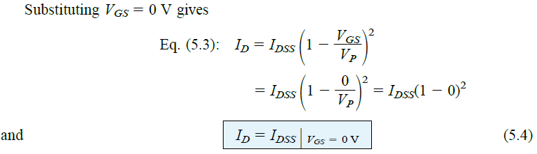
Also note that in the definitions of ID at VGS = 0 V and -1 V, the saturation level of ID is used and the ohmic region is ignored.
Going further, VGS = -2 V and -3 V, we can complete the transfer curve graph.
How to Apply the Shockley Equation
You can also obtain the transfer curve of Figure 5.3 directly by applying the Shockley equation (Equation 5.15), given the values of IDSS and Vp.
The IDSS and VP levels define the curve limits for both axes, and only a few intermediate points need to be plotted.
Shockley equation Eq.5.3 as Figure 5.15
The truth of the origin of the transfer curve can be perfectly expressed by examining certain unique levels of a particular variable and then identifying the corresponding levels of another variable by:
This matches the graph shown in Figure 5.15.
Observe how the negative signs of VGS and VP are carefully managed in the above calculations. Missing even one negative sign can lead to completely wrong results.
From the above discussion, it is clear that if we have the values of IDSS and VP (which can be referenced from the datasheet), we can quickly determine the value of ID for any magnitude of VGS.
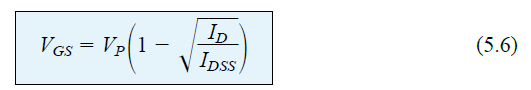
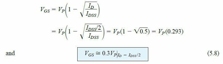
On the other hand, through standard algebra, we can derive an equation (via Equation 5.3) for the resulting VGS level for a given ID level.
This can be deduced very simply to obtain:
Now, let us verify the above formula by determining the VGS level that produces a MOSFET with a drain current of 4.5 mA and a characteristic matching that of Figure 5.15.
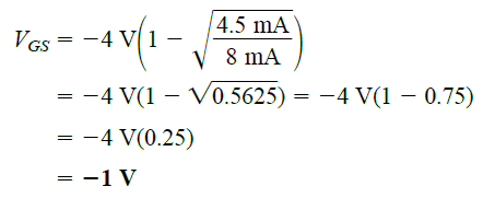
The result verifies the equation since it agrees with Figure 5.15.
Using shorthand method
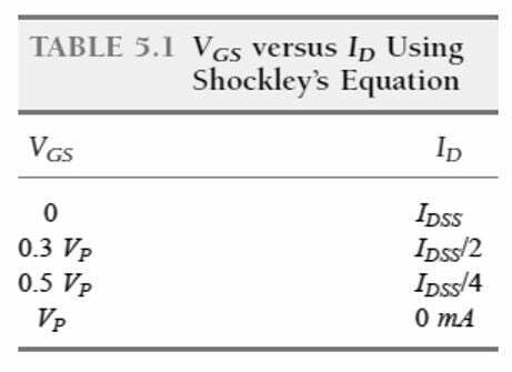
Since we need to draw transfer curves frequently, we may find it convenient to have a shorthand technique for drawing the curves. An ideal method would allow the user to draw the curve quickly and efficiently without compromising accuracy.
Equation 5.3, which we learned above, is designed in such a way that specific VGS levels produce ID levels that can be remembered for use as plotting points when plotting the transfer curve.
With VGS specified as 1/2 the pinch-off value VP, the resulting ID level can be determined using the Shockley equation as follows:
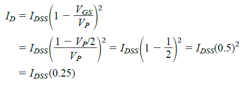
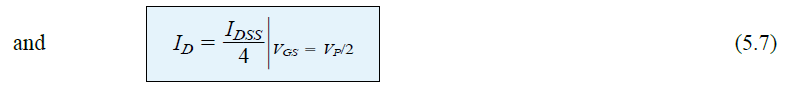
It must be noted that the above equation is not created for a specific level of VP. This equation is a general form for all VP levels, as long as VGS = VP /
2. The result of this equation shows that as long as the gate-to-source voltage is 1% less than the pinch-off value, the drain current will always be 4/50 of the saturation level IDSS.
Please note that the ID level of VGS = VP/2 = -4V/2 = -2V as shown in Figure 5.15
Choosing ID = IDSS/2 and substituting it into equation 5.6, we obtain the following result:
Although more numerical points can be established, a sufficient level of accuracy can be achieved simply by plotting the transfer curve using only 4 plot points, as shown above and in Table 5.1 below.
In most cases we can use just the plot points using VGS = VP/2 and the axis intersection at IDSS and VP will give us a curve that is reliable enough for most analyses.
- The unidirectional conduction current of the diode, the diode and its common uses
- Why do we need a MOSFET gate resistor? MOSFET Gate Resistor Placement
- What factors are related to the hysteresis loss of the transformer? Can the hysteresis loss be reduced?
- How to identify common mode interference? Methods to eliminate common mode interference
- Classification and characteristics of operational amplifiers, classification and characteristics of operational amplifiers
- Working principle/advantages/disadvantages/size of optical fiber
- DIY a decorative lamp
- Ceramic filter structure/working principle/characteristics/application
- What is a Demultiplexer
- Experiment and production of NE555 time base integrated circuit
- 555 square wave oscillation circuit
- 555 photo exposure timer circuit diagram
- Introducing the CD4013 washing machine timer circuit diagram
- Simple level conversion circuit diagram
- 555 electronic guide speaker circuit diagram for blind people
- Circuit diagram of disconnection alarm composed of 555
- Analog circuit corrector circuit diagram
- color discrimination circuit
- Color sensor amplification circuit
- Level indication circuit


 京公网安备 11010802033920号