Load transient response test of voltage regulator(1)
Source: InternetPublisher:柯南道尔 Keywords: Voltage regulator load transient response Updated: 2025/09/30
Semiconductor memory, card readers, microprocessors, disk drives, piezoelectric devices, and digital systems generate transient loads that voltage regulators must service. Ideally, the regulator output should be constant during a load transient. However, in practice, some variation occurs, and this variation can become problematic if the system exceeds its permitted operating voltage tolerance. This issue requires testing the regulator and its associated support components to verify the required performance under transient load conditions. Various methods can be used to generate transient loads and observe the regulator's response.
Figure 1 shows a conceptual load transient generator. The regulator under test drives DC and switched resistive loads, which can be manually adjusted. The device monitors its switch current and output voltage, allowing comparison of output voltage and load current under both static and dynamic conditions. The switch current is either on or off; there is no electrically controlled linear region.
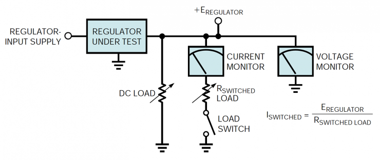
Figure 1. This concept of a voltage regulator load tester includes a switching and DC load, along with voltage and current monitors. Resistor values set the DC and switching load currents. The switch current is either on or off; there is no controllable linear region.
Figure 2 shows a practical implementation of a load transient generator. Capacitors are added to the voltage regulator under test; these capacitors provide an energy reservoir, similar to a mechanical flywheel, to aid transient response. The size, dielectric, and placement of these capacitors, especially COUT, have a significant impact on transient response and overall regulator stability (References 1 and 2). An input pulse triggers the LTC1693 FET driver to switch Q1, generating a transient load current from the regulator. An oscilloscope monitors the instantaneous load voltage, and the current is monitored via a "clip-on" broadband probe.
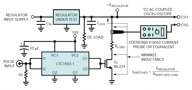
Figure 2. A practical regulator load tester includes a FET driver and switch Q1. An oscilloscope monitors the current probe output and the regulator response.
Figure 3 evaluates the circuit's load transient generation capability by replacing the regulator with a low-impedance power supply. A high-capacity power supply, low-impedance connections, and ample bypassing combine to maintain low impedance across the entire frequency range. Figure 4 shows the circuit in Figure 3 responding to an LTC1693-1 FET driver (Trace A), which cleanly switches 1A in 15 nanoseconds (Trace B). This speed is useful for simulating many loads, but its versatility is limited. While fast, the circuit cannot simulate loads between minimum and maximum currents.
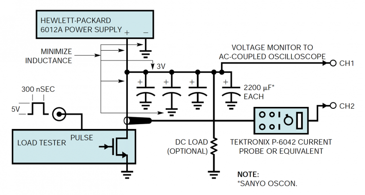
Figure 3 By replacing the regulator with a well-bypassed, low-impedance power supply, you can determine the response time of the load tester.

Figure 4 The circuit of Figure 2 responds to the output of the FET driver (trace A) by switching a 1A load (trace B) in 15 nanoseconds.
Closed-loop tester
The conceptual closed-loop load transient generator in Figure 5 linearly controls Q1's gate voltage to set an instantaneous transient current at any desired point, enabling simulation of virtually any load profile. Feedback from Q1's source to A1's control amplifier closes the loop around Q1, stabilizing its operating point. Q1's current value depends on the control input voltage and current-sense resistor within a wide bandwidth. Once A1 is biased to Q1's conductance threshold, small changes in A1's output result in large current changes in Q1's channel. Therefore, A1 does not need to have large output excursions; its small-signal bandwidth, not its slew rate, is the fundamental speed limitation. Within this limit, Q1's current waveform is identical to A1's control input voltage waveform, allowing linear control of the load current. This versatile capability allows for a wide variety of simulated loads.
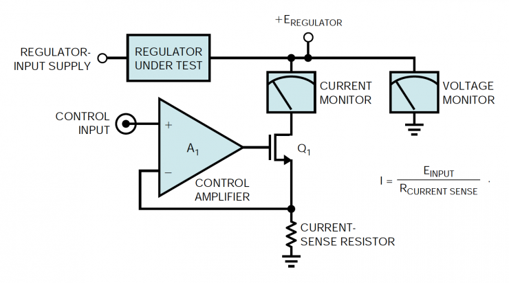
Figure 5. In this conceptual closed-loop load tester, A1 controls Q1's source voltage, setting the regulator's output current. Q1's drain current waveform is identical to A1's input, allowing linear control of the load current. The voltage and current monitors match those in Figure 1.
FET-based circuits
Figure 6 shows a practical example of a FET-based closed-loop load transient generator, including DC bias and waveform input. A1 must drive the high-capacitance gate of Q1 at high frequencies, requiring a high peak A1 output current and careful attention to feedback loop compensation. A1 is a 60MHz current feedback amplifier with an output current capability exceeding 1A. Maintaining high-frequency stability and waveform fidelity while driving Q1's gate capacitance requires settable gate drive peak components, a damping network, feedback trimming, and loop peaking adjustments. You first make the required DC trimming. With no input applied, adjust the 1mV trim at Q1 to source 1mV DC. You can use the arrangement in Figure 7 for AC trimming. Similar to the circuit in Figure 3, this "brick-wall" regulated source provides minimal ripple and droop when the load transient generator is subjected to a load step. Apply the input as shown and fine-tune the gate drive, feedback, and loop peaking adjustments to obtain the cleanest, square-corner response on the oscilloscope's current-probe-equipped channel.
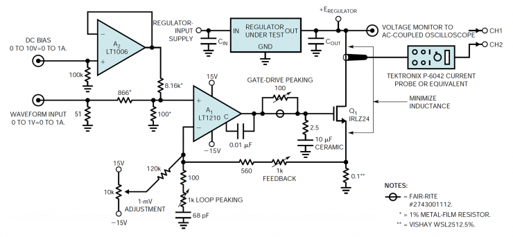
Figure 6: In a detailed closed-loop load tester, DC level and pulse inputs feed A1 to the Q1 current-sinking regulator load. Q1's gain allows for a small A1 output swing, thus allowing for a wide bandwidth. The damper network, feedback, and peak trimming optimize the edge response.
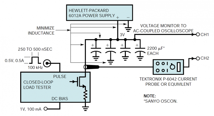
Figure 7 determines the closed-loop load tester response time as shown in Figure 3. The "brick wall" input provides a low impedance source.
- 50V 3A regulated power supply (using 2N3055)
- Electronic fuse
- 0-28V 20A Adjustable Power Supply (Based on LM317 and 2N3055)
- 500W 12V to 220V inverter
- Simple lithium-ion/lithium polymer battery charger
- A classic linear 5V power supply using a 6.3V AC transformer.
- Simple DC-AC Inverter
- USB-powered lithium-ion battery charger
- Tips on how to optimize voltage monitors
- When debugging a boost converter, you can analyze it from four directions.
- Importance of Voltage Supervisors and Output Topology Selection
- Design of adjustable DC stabilized power supply circuit module
- Power circuit of LBO-522 dual trace oscilloscope
- Power circuit with smoothing filter capacitor
- 500A-6V single-phase thyristor voltage regulating electroplating power supply circuit
- 300A-18V three-phase thyristor voltage regulating electrolytic power supply circuit
- Household emergency power circuit
- Inverter power circuit made with BJ50A
- Based on LM117 variable voltage regulator
- 5V voltage regulator circuit


 京公网安备 11010802033920号