Gate resistor and bleeder resistor
Source: InternetPublisher:aytwartoofyoroo Keywords: Resistors gate resistors bleeder resistors Updated: 2025/08/08
A resistor is added between the gate and source of a field effect transistor. What is the function of this resistor?
One is to provide bias voltage for the field effect tube; the second is to act as a discharge resistor: to protect the gate G-source S; the first function is easy to understand, here is to explain the principle of the second function - to protect the gate G-source S: the resistance value between the GS poles of the field effect tube is very large, so as long as there is a small amount of static electricity, a very high voltage will be generated at both ends of the equivalent capacitor between its GS poles. If these small amounts of static electricity are not discharged in time, the high voltage at both ends may cause the field effect tube to malfunction, or even break down its GS pole; at this time, the resistor added between the gate and the source can discharge the above-mentioned static electricity, thereby protecting the field effect tube.
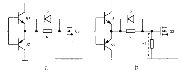
Let's take a specific example: When the MOS transistor is operating in the switching state, Q1 and Q2 are turned on in turn, and the MOS transistor gate is repeatedly charging and discharging. If the power is turned off at this time, the MOS transistor gate has two states: one is the discharge state, in which the gate equivalent capacitance has no charge stored; the other is the charge state, in which the gate equivalent capacitance is fully charged, as shown in Figure a below. Although the power is cut off, Q1 and Q2 are also in the disconnected state, and there is no circuit for charge to be released, the electric field of the MOS transistor gate still exists (and can be maintained for a long time), and the conditions for establishing a conductive channel have not disappeared. Therefore, at the moment of restarting the power supply, because the excitation signal has not yet been established, the drain power supply (V1) of the MOS transistor is randomly provided at the moment of startup. Under the action of the conductive channel, the MOS transistor immediately generates an uncontrolled large drain current Id, causing the MOS transistor to burn out. In order to avoid this phenomenon, a discharge resistor R1 is connected in parallel between the gate and source of the MOS tube, as shown in Figure b below. After shutdown, the charge stored in the gate is quickly released through R1. The resistance of this resistor should not be too large to ensure the rapid release of charge, generally around 5 kilohms to tens of kilohms.
The perfusion circuit is mainly designed to address the capacitive input characteristics of the MOS tube when it is used as a switch, which causes a lag in the "open" and "close" actions. When the MOS tube is used for other purposes, such as linear amplification, there is no need to set up a perfusion circuit.
- Infrared proximity sensor
- The Dangers of Deep Rebound ESD Circuit Protection Diodes
- Operational amplifier structure, internal circuit of f007 integrated operational amplifier
- Diode and gate circuit schematic diagram and principle analysis
- Constant voltage drop model of diode
- H-bridge drive circuit principle
- Using AD8307 logarithmic amplifier to form a power meter circuit
- Fly-Buck knowledge and circuit layout
- How to understand operational amplifiers in a simple and easy way
- Calculating the Input Impedance of a Differential Amplifier
- 555 square wave oscillation circuit
- 555 photo exposure timer circuit diagram
- Introducing the CD4013 washing machine timer circuit diagram
- Simple level conversion circuit diagram
- 555 electronic guide speaker circuit diagram for blind people
- Circuit diagram of disconnection alarm composed of 555
- Analog circuit corrector circuit diagram
- color discrimination circuit
- Color sensor amplification circuit
- Level indication circuit


 京公网安备 11010802033920号