SB570 - SB5100
5.0A SCHOTTKY BARRIER RECTIFIER
Features
·
·
·
·
·
·
·
Guard Ring Die Construction for
Transient Protection
Low Power Loss, High Efficiency
High Surge Capability
High Current Capability
Surge Overload Rating to 150A Peak
For Use in Low Voltage, High Frequency Inverters, Free
Wheeling, and Polarity Protection Applications
Lead Free Finish, RoHS Compliant (Note 2)
A
B
A
C
D
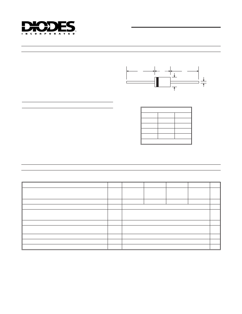
Mechanical Data
·
·
·
·
·
·
·
·
Case: DO-201AD
Case Material: Molded Plastic. UL Flammability
Classification Rating 94V-0
Moisture Sensitivity: Level 1 per J-STD-020C
Terminals: Finish - Bright Tin. Plated Leads Solderable per
MIL-STD-202, Method 208
Polarity: Cathode Band
Ordering Information: See Last Page
Marking: Type Number
Weight: 1.1 grams (approximate)
Dim
A
B
C
D
DO-201AD
Min
25.40
7.20
1.20
4.80
Max
¾
9.50
1.30
5.30
All Dimensions in mm
Maximum Ratings and Electrical Characteristics
Single phase, half wave, 60Hz, resistive or inductive load.
For capacitive load, derate current by 20%.
Characteristic
Peak Repetitive Reverse Voltage
Working Peak Reverse Voltage
DC Blocking Voltage
RMS Reverse Voltage
Average Rectified Output Current
@ T
L
= 80°C
Non-Repetitive Peak Forward Surge Current 8.3ms
single half sine-wave superimposed on rated load
(JEDEC Method)
Forward Voltage
@ I
F
= 5.0A
Peak Reverse Current
at Rated DC Blocking Voltage
Typical Junction Capacitance
Typical Thermal Resistance Junction to Ambient
Operating and Storage Temperature Range
Notes:
@ T
A
= 25°C unless otherwise specified
Symbol
V
RRM
V
RWM
V
R
V
R(RMS)
I
O
I
FSM
V
FM
I
RM
C
j
R
qJA
T
j,
T
STG
SB570
70
49
SB580
80
56
5.0
150
0.80
0.5
50
400
10
SB590
90
63
SB5100
100
70
Unit
V
V
A
A
V
mA
pF
K/W
°C
@ T
A
= 25°C
@ T
A
= 100°C
(Note 1)
-65 to +150
1. Measured at 1.0MHz and applied reverse voltage of 4.0V DC.
2. RoHS revision 13.2.2003. Glass and High Temperature Solder Exemptions Applied, see
EU Directive Annex Notes 5 and 7.
DS30135 Rev. 5 - 2
1 of 3
www.diodes.com
SB570 - SB5100
ã
Diodes Incorporated
Resistive or
Inductive Load
4
I
F
, INSTANTANEOUS FORWARD CURRENT (A)
5
40
I
(AV),
AVERAGE FORWARD CURRENT (A)
10
3
2
T
A
= 100
°
C
1.0
1
T
A
= 25
°
C
0
0
25
50
75
100
125
150
0.1
0
0.2
0.4
0.6
0.8
1.0
V
F
, INSTANTANEOUS FORWARD VOLTAGE (V)
Fig. 2 Typical Forward Characteristics
T
L
, LEAD TEMPERATURE (
°
C)
Fig. 1 Forward Current Derating Curve
I
FSM
, PEAK FORWARD SURGE CURRENT (A)
150
Single Half-Sine-Wave
(JEDEC Method)
1000
T
A
= 25°C
f = 1.0 Mhz
120
C
j
, CAPACITANCE (pF)
90
100
60
30
0
1
10
100
NUMBER OF CYCLES AT 60Hz
Fig. 3 Max Non-Repetitive Peak Fwd Surge Current
I
R
, INSTANTANEOUS REVERSE CURRENT (mA)
10
10
0.1
10
V
R
, REVERSE VOLTAGE (V)
Fig. 4 Typical Junction Capacitance
1
100
1
T
A
= 100
°
C
0.1
T
A
= 75
°
C
0.01
T
A
= 25
°
C
0.001
T
A
= -25
°
C
0.0001
0
20
40
60
80
100
120
140
PERCENT OF RATED PEAK REVERSE VOLTAGE (%)
Fig. 5 Typical Reverse Characteristics
DS30135 Rev. 5 - 2
2 of 3
www.diodes.com
SB570 - SB5100
Ordering Information
(Note 3)
Device
SB570-B
SB570-T
SB580-B
SB580-T
SB590-B
SB590-T
SB5100-B
SB5100-T
Notes:
Packaging
DO-201AD
DO-201AD
DO-201AD
DO-201AD
DO-201AD
DO-201AD
DO-201AD
DO-201AD
Shipping
500/Bulk
1.2K/Tape & Reel, 13-inch
500/Bulk
1.2K/Tape & Reel, 13-inch
500/Bulk
1.2K/Tape & Reel, 13-inch
500/Bulk
1.2K/Tape & Reel, 13-inch
3. For packaging details, visit our website at http://www.diodes.com/datasheets/ap02008.pdf.
DS30135 Rev. 5 - 2
3 of 3
www.diodes.com
SB570 - SB5100
 京公网安备 11010802033920号


