EEWORLDEEWORLDEEWORLD

Part Number

Search

MPSL01

Description
RF SMALL SIGNAL TRANSISTOR
CategoryDiscrete semiconductor    The transistor   
File Size519KB,4 Pages
ManufacturerCentral Semiconductor
Download Datasheet Parametric Compare View All

MPSL01 Online Shopping

Suppliers Part Number Price MOQ In stock  
MPSL01 - - View Buy Now

MPSL01 Overview

RF SMALL SIGNAL TRANSISTOR

MPSL01 Parametric

Parameter NameAttribute value
Is it lead-free?Contains lead
Is it Rohs certified?incompatible
MakerCentral Semiconductor
Parts packaging codeTO-92
package instructionCYLINDRICAL, O-PBCY-T3
Contacts3
Reach Compliance Codenot_compliant
Maximum collector current (IC)0.15 A
Collector-emitter maximum voltage120 V
ConfigurationSINGLE
Minimum DC current gain (hFE)50
JEDEC-95 codeTO-92
JESD-30 codeO-PBCY-T3
JESD-609 codee0
Number of components1
Number of terminals3
Maximum operating temperature150 °C
Package body materialPLASTIC/EPOXY
Package shapeROUND
Package formCYLINDRICAL
Peak Reflow Temperature (Celsius)NOT SPECIFIED
Polarity/channel typeNPN
Maximum power dissipation(Abs)0.625 W
Certification statusNot Qualified
surface mountNO
Terminal surfaceTin/Lead (Sn/Pb)
Terminal formTHROUGH-HOLE
Terminal locationBOTTOM
Maximum time at peak reflow temperatureNOT SPECIFIED
Transistor component materialsSILICON
Nominal transition frequency (fT)60 MHz
MPSA92
MPSA93
w w w. c e n t r a l s e m i . c o m
SILICON
HIGH VOLTAGE
PNP TRANSISTORS
DESCRIPTION:
The CENTRAL SEMICONDUCTOR MPSA92 and
MPSA93 are silicon PNP transistors designed for
high voltage applications.
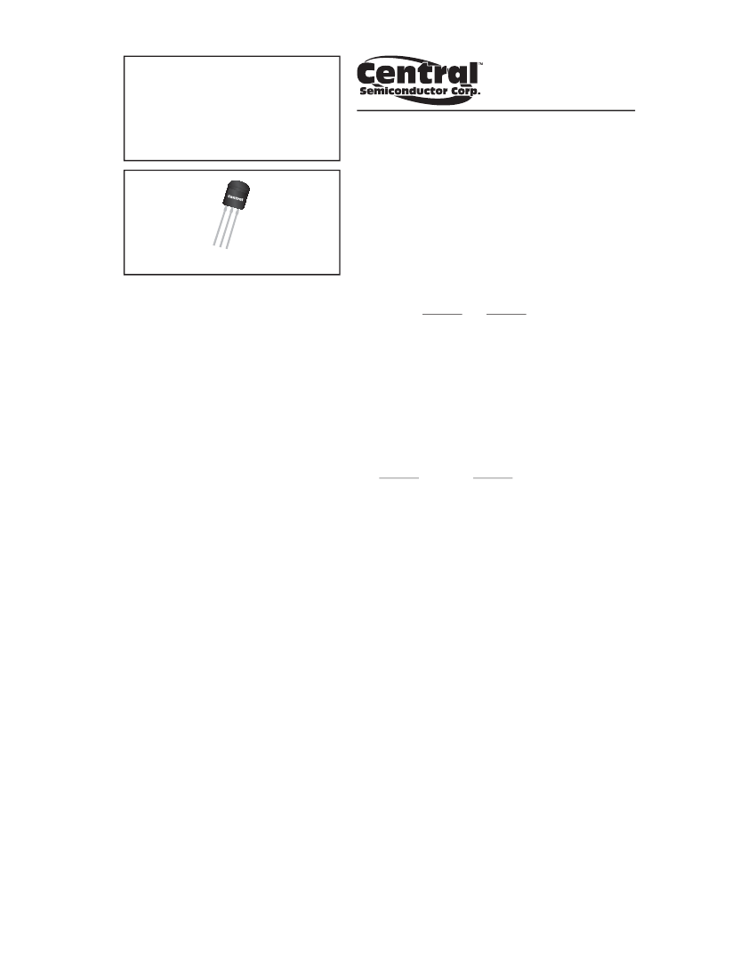
MARKING: FULL PART NUMBER
TO-92 CASE
MAXIMUM RATINGS:
(TA=25°C unless otherwise noted)
SYMBOL
Collector-Base Voltage
VCBO
Collector-Emitter Voltage
VCEO
Emitter-Base Voltage
Continuous Collector Current
Power Dissipation
Power Dissipation (TC=25°C)
Operating and Storage Junction Temperature
Thermal Resistance
Thermal Resistance
ELECTRICAL
SYMBOL
ICBO
ICEO
IEBO
BVCBO
BVCEO
BVEBO
VCE(SAT)
VBE(SAT)
hFE
hFE
hFE
fT
Cob
CHARACTERISTICS:
(TA=25°C)
TEST CONDITIONS
VCB=200V
VCE=160V
VEB=3.0V
IC=100μA
IC=1.0mA
IE=100μA
IC=20mA, IB=2.0mA
IC=20mA, IB=2.0mA
VCE=10V, IC=1.0mA
VCE=10V, IC=10mA
VCE=10V,
VCE=20V,
IC=30mA
IC=10mA, f=100MHz
VCB=20V, IE=0, f=1.0MHz
VEBO
IC
PD
PD
TJ, Tstg
JA
JC
MPSA92
MIN
MAX
-
250
-
-
300
300
5.0
-
-
25
40
25
50
-
-
100
-
-
-
0.5
0.9
-
-
-
-
6.0
MPSA92
300
300
5.0
500
625
1.5
MPSA93
200
200
UNITS
V
V
V
mA
mW
W
°C
°C/W
°C/W
-65 to +150
200
83.3
MPSA93
MIN
MAX
-
-
-
-
200
200
5.0
-
-
25
40
25
50
-
250
100
-
-
-
0.4
0.9
-
-
-
-
8.0
UNITS
nA
nA
nA
V
V
V
V
V
MHz
pF
R2 (15-December 2014)

MPSL01 Related Products

MPSL01 MPSA25 MPSA45 MPSA75 MPSA76 MPSD04 MPSD54 MPSH11 MPSL51 PN3639
Description RF SMALL SIGNAL TRANSISTOR 300,000 SYSTEM GATE 1.8V FPGA - NOT RECOMMENDED for NEW DESIGN 300,000 SYSTEM GATE 1.8V FPGA - NOT RECOMMENDED for NEW DESIGN 300,000 SYSTEM GATE 1.8V FPGA - NOT RECOMMENDED for NEW DESIGN 300,000 SYSTEM GATE 1.8V FPGA - NOT RECOMMENDED for NEW DESIGN NPN, Si, SMALL SIGNAL TRANSISTOR, TO-92 300,000 SYSTEM GATE 1.8V FPGA - NOT RECOMMENDED for NEW DESIGN 300,000 SYSTEM GATE 1.8V FPGA - NOT RECOMMENDED for NEW DESIGN 300,000 SYSTEM GATE 1.8V FPGA - NOT RECOMMENDED for NEW DESIGN 300,000 SYSTEM GATE 1.8V FPGA - NOT RECOMMENDED for NEW DESIGN
Is it lead-free? Contains lead Contains lead Contains lead Contains lead Contains lead Contains lead Contains lead Contains lead Contains lead -
Is it Rohs certified? incompatible incompatible incompatible incompatible incompatible incompatible incompatible incompatible incompatible -
Maker Central Semiconductor Central Semiconductor Central Semiconductor Central Semiconductor Central Semiconductor Central Semiconductor Central Semiconductor Central Semiconductor Central Semiconductor -
Parts packaging code TO-92 TO-92 TO-92 TO-92 TO-92 TO-92 TO-92 - TO-92 -
package instruction CYLINDRICAL, O-PBCY-T3 TO-92, 3 PIN CYLINDRICAL, O-PBCY-T3 TO-92, 3 PIN TO-92, 3 PIN TO-92, 3 PIN TO-92, 3 PIN - CYLINDRICAL, O-PBCY-T3 -
Contacts 3 3 3 3 3 3 3 - 3 -
Reach Compliance Code not_compliant unknow not_compliant _compli not_compliant _compli unknow unknow _compli -
Maximum collector current (IC) 0.15 A 0.5 A 0.3 A 0.5 A 0.5 A 0.5 A 0.5 A - 0.6 A -
Configuration SINGLE DARLINGTON SINGLE DARLINGTON DARLINGTON DARLINGTON DARLINGTON SINGLE SINGLE -
Minimum DC current gain (hFE) 50 10000 50 10000 10000 1000 1000 60 40 -
JEDEC-95 code TO-92 TO-92 TO-92 TO-92 TO-92 TO-92 TO-92 TO-92 TO-92 -
JESD-30 code O-PBCY-T3 O-PBCY-T3 O-PBCY-T3 O-PBCY-T3 O-PBCY-T3 O-PBCY-T3 O-PBCY-T3 O-PBCY-T3 O-PBCY-T3 -
JESD-609 code e0 e0 e0 e0 e0 e0 e0 e0 e0 -
Number of components 1 1 1 1 1 1 1 1 1 -
Number of terminals 3 3 3 3 3 3 3 3 3 -
Maximum operating temperature 150 °C 150 °C 150 °C 150 °C 150 °C 150 °C 150 °C 150 °C 150 °C -
Package body material PLASTIC/EPOXY PLASTIC/EPOXY PLASTIC/EPOXY PLASTIC/EPOXY PLASTIC/EPOXY PLASTIC/EPOXY PLASTIC/EPOXY PLASTIC/EPOXY PLASTIC/EPOXY -
Package shape ROUND ROUND ROUND ROUND ROUND ROUND ROUND ROUND ROUND -
Package form CYLINDRICAL CYLINDRICAL CYLINDRICAL CYLINDRICAL CYLINDRICAL CYLINDRICAL CYLINDRICAL CYLINDRICAL CYLINDRICAL -
Peak Reflow Temperature (Celsius) NOT SPECIFIED NOT SPECIFIED NOT SPECIFIED NOT SPECIFIED NOT SPECIFIED NOT SPECIFIED NOT SPECIFIED NOT SPECIFIED NOT SPECIFIED -
Polarity/channel type NPN NPN NPN PNP PNP NPN PNP NPN PNP -
Maximum power dissipation(Abs) 0.625 W - 0.625 W - 0.625 W 1.5 W 0.625 W 0.35 W 0.625 W -
Certification status Not Qualified Not Qualified Not Qualified Not Qualified Not Qualified Not Qualified Not Qualified Not Qualified Not Qualified -
surface mount NO NO NO NO NO NO NO NO NO -
Terminal surface Tin/Lead (Sn/Pb) Tin/Lead (Sn/Pb) Tin/Lead (Sn/Pb) Tin/Lead (Sn/Pb) Tin/Lead (Sn/Pb) Tin/Lead (Sn/Pb) Tin/Lead (Sn/Pb) Tin/Lead (Sn/Pb) Tin/Lead (Sn/Pb) -
Terminal form THROUGH-HOLE THROUGH-HOLE THROUGH-HOLE THROUGH-HOLE THROUGH-HOLE THROUGH-HOLE THROUGH-HOLE THROUGH-HOLE THROUGH-HOLE -
Terminal location BOTTOM BOTTOM BOTTOM BOTTOM BOTTOM BOTTOM BOTTOM BOTTOM BOTTOM -
Maximum time at peak reflow temperature NOT SPECIFIED NOT SPECIFIED NOT SPECIFIED NOT SPECIFIED NOT SPECIFIED NOT SPECIFIED NOT SPECIFIED NOT SPECIFIED NOT SPECIFIED -
Transistor component materials SILICON SILICON SILICON SILICON SILICON SILICON SILICON SILICON SILICON -
Nominal transition frequency (fT) 60 MHz 125 MHz 20 MHz 125 MHz 125 MHz 100 MHz 100 MHz 650 MHz 60 MHz -

EEWorld
subscription
account

EEWorld
service
account

Automotive
development
circle

Robot
development
community

Index Files: 2339  1263  1178  1416  1443  48  26  24  29  30 
Datasheet   0 1 2 3 4 5 6 7 8 9 A B C D E F G H I J K L M N O P Q R S T U V W X Y Z
Room 1530, 15th Floor, Building B, No. 18 Zhongguancun Street, Haidian District, Beijing Telephone: (010) 82350740 Postal Code: 100190
Copyright © 2005-2026 EEWORLD.com.cn, Inc. All rights reserved 京ICP证060456号 京ICP备10001474号-1 电信业务审批[2006]字第258号函 京公网安备 11010802033920号