In How to Handle High Di/dt Load Transients (Part 1), we discussed the capacitive bypass requirements of some loads when the current changes rapidly. We found it necessary to place low equivalent series inductance (ESL) capacitors close to the load because less than 0.5 nH can produce an unacceptable voltage surge. In practice, achieving this low inductance requires placing multiple bypass capacitors and multiple interconnect pins in the processor package. In this article, we will discuss the size of the bypass capacitor required to achieve the practical di/dt requirements of the power supply output.
For the convenience of discussion, Figure 1 shows the P-SPICE model of the power system. This diagram consists of the compensation circuit power supply, modulator (G1) and output capacitor. Also included internally are interconnected inductors, bypass capacitive load models, DC loads, and step loads.
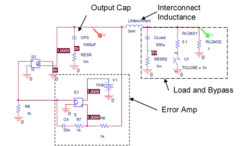
Figure 1 Simple P-SPICE model assists system design
First, you need to decide whether to treat the power supply and load as separate "black boxes" or to approach the problem as a complete power system design. If you use a system-level approach, you can use load bypass capacitors to reduce the power supply output capacitance, thereby saving system cost. If using the "black box" approach, you test the power supply and load separately. Regardless of which method you use, you need to know how much bypass capacitance your load requires.
First, estimate the size of the interconnect inductance and resistance between the source and load. This interconnect impedance (Linterconnect) forms a bypass capacitor (Cbypass) low-pass filter. We assume the power supply output impedance is low. Using the low-pass filter's characteristic impedance (ZO), load step value (Istep), and allowable voltage fluctuation (dV), establish the bypass filter requirements (Equation 1-2):
![]() Equation 1
Equation 1
![]() Equation 2
Equation 2
Solving Equation 2 gives Z0, then substituting into Equation 1 gives Equation 3:
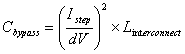 Equation 3
Interestingly, the required capacitance size is related to the square of the load current divided by the square of the allowed perturbation, so calculate these two values carefully.
Interconnect inductance can range from tens of nH for parallel power supplies, to hundreds of nHs for distantly placed power supplies. A good rule of thumb is to add about 15 nH of interconnect inductance per inch. With a load step of 10 amps and an allowed disturbance of 30mV, the bypass requirements range from 500 uF at 5 nH to 50 mF at 500 nH.
In addition, this filter reduces the rate at which the load current of the power supply rises. If the lossless filter is excited by a current square wave, the inductor current is sinusoidal. The rate of rise can be calculated by differentiating the current waveform in Equation 4-7.
![]() Equation 4
Equation 4
![]() Equation 5
Equation 5
Equation 6
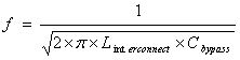 Equation 7
With an interconnect inductance of 5 nH and a bypass capacitance of 500 uF, a 10-amp step change results in a supply current rise rate of 0.2 A/uS. Larger inductance results in lower di/dt. These values are much smaller than those specified by system designers.
When using a system-level approach, maximize loop bandwidth while minimizing total capacitance. Now, think about how to use the "black box" approach. You have to allow the power supply to be stable without bypass capacitors and with the maximum expected bypass capacitance. As mentioned earlier, interconnect capacitance drives up the bypass capacitance requirements of the load. This in turn affects the capacitance of the power supply when using the "black box" approach. The connection capacitance range determines the crossover frequency range of the power supply. In both voltage and current modes, both are proportional. You can maximize the crossover frequency with no load capacitor, but as soon as a load is connected, the crossover frequency drops dramatically.
Table 1 compares the required capacitors for three interconnecting inductors in an example system. Comparative data is obtained by varying the interconnect inductance, calculating the load bypass capacitance, and designing the corresponding output stage and control loop of the power supply. Case 1 has the load and power supply placed side by side; Case 2 has a medium interconnect inductance between the power supply and the load. In case 3, the inductance of the power supply connected using the cable is extremely high. The amount of bypass required is directly related to the interconnect inductance.
In this case, case 3 is 100 times the interconnect inductance, as is the bypass capacitance. This creates ripple in the power supply design because the power supply must remain stable with and without bypass capacitors. Obviously the first method is better because it uses the fewest capacitors and costs the least. In case 2, the interconnection inductance is controlled to a certain extent and the number of capacitors is increased to a certain extent. In Case 3, the large number of interconnected inductors creates serious cost issues. Case 2 and Case 3 also have a benefit: independent power supply testing.

Table 1 Leveraging a system-level approach to reduce power system costs
Figure 2 compares simulated output voltage changes during load transients for small and large interconnect inductances. The response of a small inductor gradually weakens quickly, but this is not the case for a large inductor, which takes a longer time to stabilize. This is due to higher characteristic impedance and lower resonant frequency. In addition, if the load current jumps regularly at this resonant frequency, extremely wide and damaging voltage changes will occur.

Figure 2 Voltage ringing becomes a problem with large interconnect inductance
In summary, high di/dt loads require careful bypass design to maintain dynamic regulation of the power supply. Low-inductance interconnects must be used between the load and the bypass capacitor and between the bypass capacitor and the load. A system-level approach enables a lowest-cost solution. For the convenience of system testing, many system engineers ignore this cost-saving solution by reducing power supply capacitance.
In the future, we will discuss some empirical conclusions to determine the optimal gate drive timing scheme for synchronous buck architecture, so stay tuned.
You Might Like
Recommended Posts
EEWorld
subscription
account

EEWorld
service
account

Automotive
development
circle

About Us Customer Service Contact Information Datasheet Sitemap LatestNews


Room 1530, 15th Floor, Building B,
No.18 Zhongguancun Street,
Haidian District,
Beijing, Postal Code: 100190
China
Telephone: 008610 8235 0740
 京公网安备 11010802033920号
