A money counting machine is a device that automatically counts banknotes. As the scale of cash circulation becomes larger and larger, the level of counterfeit banknote manufacturing is getting higher and higher, requiring banknote counting machines to integrate counting and counterfeit identification, and continuously improving the counterfeit detection performance of banknote counting machines. According to the new regulations issued by GB16999-2010 "General Technical Conditions for RMB Discriminators", the new national mandatory standard for banknote counting machines has added the counterfeiting level indicator of RMB discriminators. For the first time, banknote counting machines are divided into 3 different levels, namely A There are three grades, B and C. Among them, Class A and B are the bank currency counting and inspection machine grades, and Class C is the commercial currency counting and inspection machine grade. Class A banknote counting machines must have more than 9 identification capabilities/identification technologies.
This reference design provides a banknote counting machine solution based on CIS sensors, which can implement identification technologies such as white light image analysis, infrared light image analysis, edge image processing (with related algorithms, serial number recognition can be achieved).
The DSP uses the ADSP-BF609 Blackfin processor, which is optimized for embedded vision and video analysis applications, using a dual-core fixed-point DSP processor and a unique Pipeline Vision Processor (PVP), designed to speed up image processing algorithms and reduce overall bandwidth requirements And design.
CIS analog front end: The high-speed design uses ADDI7006, which can provide 6 channels of 10-bit analog-to-digital conversion, up to 40MSPS per channel; the low-speed design uses AD9826/AD9822, which can provide 3 channels of 16-bit analog-to-digital conversion, up to 5MSPS per channel.
The complete information includes the following content:
1. Product user manual
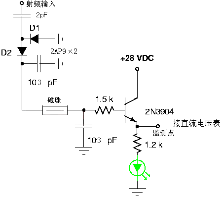
2. CIS sensor and AD9826/ADDI7006 hardware schematic diagram
3. DSP hardware schematic diagram
4. FPGA hardware schematic diagram


Blockdiagram
All reference designs on this site are sourced from major semiconductor manufacturers or collected online for learning and research. The copyright belongs to the semiconductor manufacturer or the original author. If you believe that the reference design of this site infringes upon your relevant rights and interests, please send us a rights notice. As a neutral platform service provider, we will take measures to delete the relevant content in accordance with relevant laws after receiving the relevant notice from the rights holder. Please send relevant notifications to email: bbs_service@eeworld.com.cn.
It is your responsibility to test the circuit yourself and determine its suitability for you. EEWorld will not be liable for direct, indirect, special, incidental, consequential or punitive damages arising from any cause or anything connected to any reference design used.
Supported by EEWorld Datasheet
EEWorld
subscription
account

EEWorld
service
account

Automotive
development
community

Robot
development
community

About Us Customer Service Contact Information Datasheet Sitemap LatestNews


Room 1530, 15th Floor, Building B,
No.18 Zhongguancun Street,
Haidian District,
Beijing, Postal Code: 100190
China
Telephone: 008610 8235 0740
 京公网安备 11010802033920号

 CXL5001M