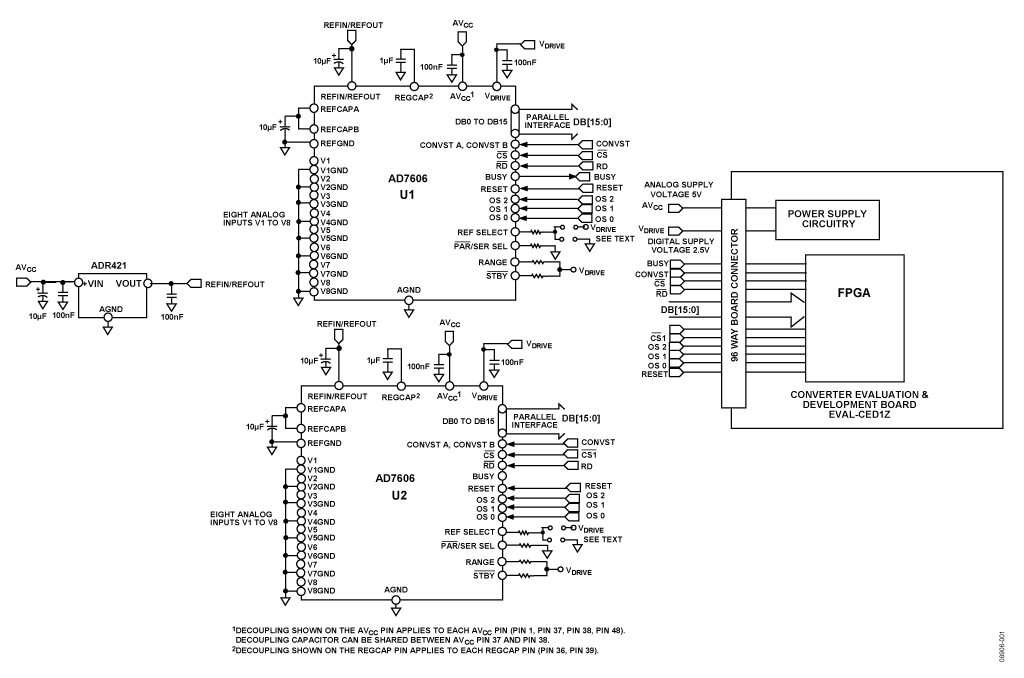
In power line measurement and protection systems, a large number of current and voltage channels in a multiphase transmission and distribution network need to be sampled simultaneously. In these applications, the number of channels ranges from 6 to more than 64. The AD7606 8-channel data acquisition system (DAS) integrates a 16-bit bipolar simultaneous sampling SAR ADC and on-chip overvoltage protection functions, which can greatly simplify the signal conditioning circuit and reduce the number of components, circuit board area, and measurement protection board costs. The high level of integration allows each AD7606 to operate with only nine low-value ceramic decoupling capacitors.
In measurement and protection systems, simultaneous sampling capabilities are necessary to maintain phase information between current and voltage channels in multiphase power line networks. The AD7606's wide dynamic range makes it an ideal device for capturing undervoltage/undercurrent and overvoltage/overcurrent conditions. The input voltage range is pin-programmable to ±5 V or ±10 V.
This circuit note details the recommended printed circuit board (PCB) layout for applications using multiple AD7606 devices. The layout is optimized for channel-to-channel matching and device-to-device matching, helping to simplify the calibration procedure for high-channel-count systems. When channel-to-channel matching is important, this circuit can use the 2.5 V internal AD7606 reference; for high-channel-count applications requiring excellent absolute accuracy, this circuit can use the external precision ADR421 reference , which has high accuracy (Class B : ±1 mV maximum), low drift (Grade B: 3 ppm/°C maximum), low noise (1.75 μV pp typical, 0.1 Hz to 10 Hz) and other characteristics. Low noise and excellent stability and accuracy make the ADR421 ideal for high-precision conversion applications. Combined, these two devices enable a level of integration, channel density and accuracy unprecedented in the industry.
The AD7606 is an integrated 8-channel data acquisition system with on-chip input amplifier, overvoltage protection circuitry, second-order analog anti-aliasing filter, analog multiplexer, 16-bit 200 kSPS SAR ADC and a digital filter . The circuit shown in Figure 1 includes two AD7606 devices and can be configured to use the 2.5 V internal reference or the ADR421 2.5 V external reference. If the REF SELECT pin is tied to a logic high level, the internal reference voltage source is selected. If the REF SELECT pin is tied to a logic low, the external reference voltage source is selected.
Power requirements are as follows: AV CC = 5 V, V DRIVE = 2.3 V to 5 V (depending on external logic interface requirements).
This circuit note describes the layout and performance of an evaluation board containing two AD7606s forming a 16-channel data acquisition system. To view the complete 16-channel DAS PC board documentation, please visit: www.analog.com/CN0148_PCB_Documentation
To achieve good channel-to-channel and device-to-device matching, a symmetrical layout of analog input channels and device decoupling is important. The data shown supports the matching performance achieved with the 16-channel ADC shown in Figure 1.

Dual AD7606 board layout for 16-channel DAS
In a system containing multiple AD7606 devices, the devices must be laid out symmetrically to ensure good performance matching between the devices. Figure 2 shows a layout using two AD7606 devices.


The AV CC voltage plane is routed along the right side of the two devices, and the V DRIVE power trace is routed along the left side of the two AD7606 devices. The reference voltage chip ADR421 is located between the two AD7606 devices. The reference voltage trace is routed upward to pin 42 of U2 and downward to pin 42 of U1. Use a solid ground plane. These symmetrical layout guidelines apply to systems containing more than two AD7606 devices. The AD7606 device can be placed in the north-south direction, with the reference voltage in the middle of the device, and the reference voltage traces laid out in the north-south direction, similar to Figure 2.
Good decoupling is also important in order to reduce the supply impedance of the AD7606, as well as the amplitude of its supply spikes. Decoupling capacitors should be placed close to (ideally right next to) these pins and their corresponding ground pins.
The decoupling capacitors of the REFIN/REFOUT pins and the REFCAPA and REFCAPB pins are important capacitors related to performance and should be as close as possible to the corresponding AD7606 pins. If possible, these capacitors should be placed on the same side of the board as the AD7606 device. Figure 3 shows the recommended decoupling configuration for the top layer of the AD7606 circuit board. The four ceramic capacitors shown are decoupling capacitors for the REFIN/REFOUT pin, REGCAP pin, REFCAPA pin, and REFCAPB pin. These capacitors are placed in a north-south direction so as to be as close as possible to the corresponding pins.


Figure 4 shows the low-level decoupling configuration, which is used to decouple the four AVCC pins and the VDRIVE pin. Use multiple vias to connect the pins to their corresponding decoupling capacitors. The symmetrical layout of decoupling capacitors around the AD7606 device facilitates performance matching between devices. Multiple vias are used to connect capacitor pads and pin pads to ground and to voltage planes and reference voltage traces.


Channel-to-channel matching for 16-channel systems
In high-channel-count systems, good channel-to-channel and device-to-device performance matching can greatly simplify the calibration procedure. The symmetrical layout of the AD7606 device, analog input channels, and decoupling capacitors helps match performance between multiple devices. Using a common system reference voltage will further enhance the matching performance of the system. Figure 5 shows the circuit configuration used to measure performance matching among the 16 channels on the board with all inputs tied to ground. There is also a distribution histogram of up to 7 codes, and the center of each channel histogram is code 0, as shown in Figure 6.


AD7606 internal voltage reference used as system reference
AD7606 has a built-in 2.5 V reference voltage source. After internal amplification, it can provide a buffer reference voltage of approximately 4.5 V for the AD7606 ADC. In high-channel-count applications where channel-to-channel and device-to-device matching are critical, the internal reference of one AD7606 can be used to provide the reference voltage for another AD7606 device. In this configuration, U1 is configured to operate from the internal reference voltage, as shown in Figure 7.


The AD7606 U2 device can be configured to operate in external reference mode. The 2.5 V reference voltage provided by the U1 REFIN/RFOUT pin is routed to the U2 REFIN/REFOUT pin. A 10 μF decoupling capacitor is located at the REFIN/REFOUT pin of the AD7606 device. On the AD7606 U1 and U2, the REFCAPA and REFCAPB pins are shorted together and decoupled to GND with a 10 μF ceramic capacitor.
Both AD7606 devices are operating at a sampling rate of 200 kSPS, with a 7.5 V DC signal applied to V1 and V2 of U1, as shown in Figure 7. The histogram of the code is shown in Figure 8. Between channels of the same device, the average output code differs by 1.2 codes. All 16 channels on the board convert at 200 kSPS.


A 7.5 V signal is applied to V1 of U1 and V1 of U2, and all 16 channels on the board operate at 200 kSPS, as shown in the configuration circuit schematic of Figure 9. The histogram of the code is shown in Figure 10. Between the V1 channels of different devices, the average output codes differ by 1.4 codes.


When using one of the AD7606's internal references as the system reference, the above histogram shows very good matching between channels of an AD7606 device and between channels of multiple devices.
absolute accuracy
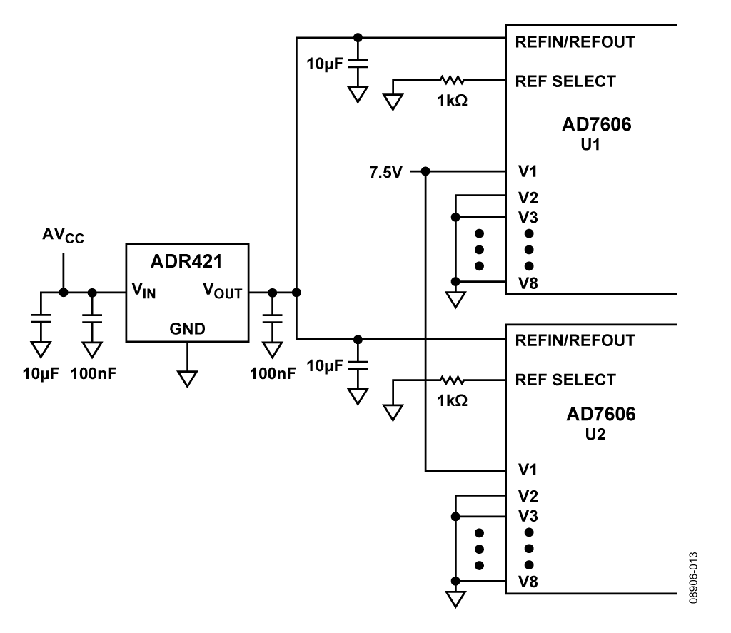
In addition to channel-to-channel matching and device-to-device matching, if the absolute accuracy of the ADC conversion results is also very important, an external small-tolerance, low-drift reference voltage source should be used as the system reference voltage source. In this circuit, the ADR421 2.5 V reference is used as the system reference.
The reference voltage applied to the AD7606 device affects the ADC output code:

The actual ideal code value will vary with temperature, depending on the temperature coefficient characteristics of the system reference. In applications where absolute accuracy is important, or where it is desired to avoid complex temperature calibration procedures to achieve absolute accuracy and channel matching, a small tolerance, low drift 2.5 V reference such as the ADR421 should be used as the system reference for the AD7606 device power source.
A 7.5 V DC voltage is applied to the inputs of U1 (V1 and V2), as shown in the circuit of Figure 11, and an external reference voltage source is used. The code histograms of the two channels of U1 are shown in Figure 12. The average code histograms of the two channels differ by 0.9 LSB.


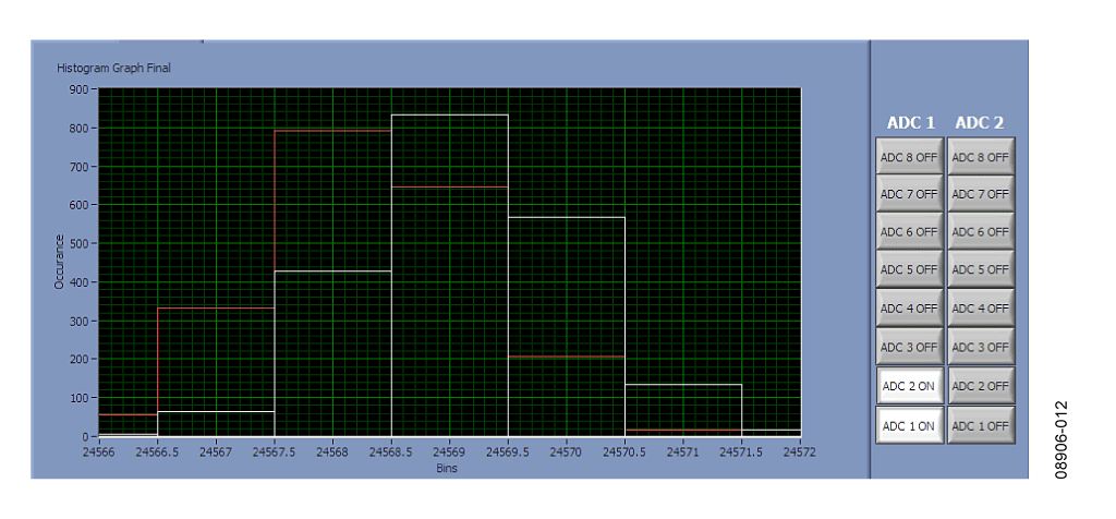
In the circuit shown in Figure 13 for testing device-to-device matching, a 7.5 V DC signal is applied to the V1 channel of the U1 and U2 AD7606 devices using an external reference. The code histograms for the two V1 channels of the two AD7606 devices are shown in Figure 14. All 16 channels on the board operate at 200 kSPS throughput rate. The code histogram averages differ by 0.6 LSB between the V1 channels of U1 and U2.


The above histogram shows that when using the ADR421 external system reference, the match between the histogram averages of one AD7606 device and the match of the histogram averages of multiple AD7606 devices are both less than 1 LSB.
in conclusion
This layout ensures good channel-to-channel matching with one AD7606, and good device-to-device matching between multiple AD7606s on the same PC board. The symmetrical layout of the AD7606 device, especially the decoupling capacitors, will help achieve good channel-to-channel matching and device-to-device matching. In high-channel-count systems, good channel-to-channel and device-to-device performance matching means calibration procedures are simplified.

Blockdiagram
All reference designs on this site are sourced from major semiconductor manufacturers or collected online for learning and research. The copyright belongs to the semiconductor manufacturer or the original author. If you believe that the reference design of this site infringes upon your relevant rights and interests, please send us a rights notice. As a neutral platform service provider, we will take measures to delete the relevant content in accordance with relevant laws after receiving the relevant notice from the rights holder. Please send relevant notifications to email: bbs_service@eeworld.com.cn.
It is your responsibility to test the circuit yourself and determine its suitability for you. EEWorld will not be liable for direct, indirect, special, incidental, consequential or punitive damages arising from any cause or anything connected to any reference design used.
Supported by EEWorld Datasheet
EEWorld
subscription
account

EEWorld
service
account

Automotive
development
community

Robot
development
community

About Us Customer Service Contact Information Datasheet Sitemap LatestNews


Room 1530, 15th Floor, Building B,
No.18 Zhongguancun Street,
Haidian District,
Beijing, Postal Code: 100190
China
Telephone: 008610 8235 0740
 京公网安备 11010802033920号

 TMT12-221S-5.0-TZZ02