Ideally, wireless measurement nodes have low power consumption, long range, and are easy to interface with different sensors. By using ADI's three devices together, it is possible to achieve an intelligent measurement node with an average current consumption of <70 μA, a distance of nearly 1 km (without obstacles), and a data rate of one transmission per minute, while maintaining 16-bit ADC performance (see Figure 1 ), making the circuit suitable for battery-powered and automation, remote detection and other applications.
The low-power temperature measurement node included in the system wakes up once every minute, measures the temperature and sends the results to the base node at 10 kbps, then returns to sleep. The base node continuously receives data packets from the measurement node and sends the information to the PC via UART for display within the "HyperTerminal".
The ADUC7060 precision analog microcontroller uses a low-power ARM7 core and has a variety of precision analog functions. Thanks to the built-in on-chip multiplexer, digital programmable gain amplifier (PGA), voltage reference, programmable current source, and 24-bit Σ-Δ ADC, the device can interface directly with virtually any temperature and bridge sensor. In this example, a 4-wire Pt100 (100 Ω platinum RTD) temperature sensor was selected. For details on the measurement circuit, see Application Note Application Note AN-0970. The wireless frequency band selected for this application is the license-exempt ISM (Industrial, Scientific and Medical) band below 1GHz. The ADF7021 transceiver supports frequency bands ranging from 431 MHz to 478 MHz and 862 MHz to 956 MHz, making it a natural choice. This low-power transceiver requires minimal external components and easily interfaces with the ADuC7060 precision analog microcontroller for excellent performance.
The ADP121 voltage regulator provides a 2.5 V supply voltage from two 1.5 V batteries. The regulator's extremely low quiescent current (11 μA at no load) is critical to maximizing battery life.

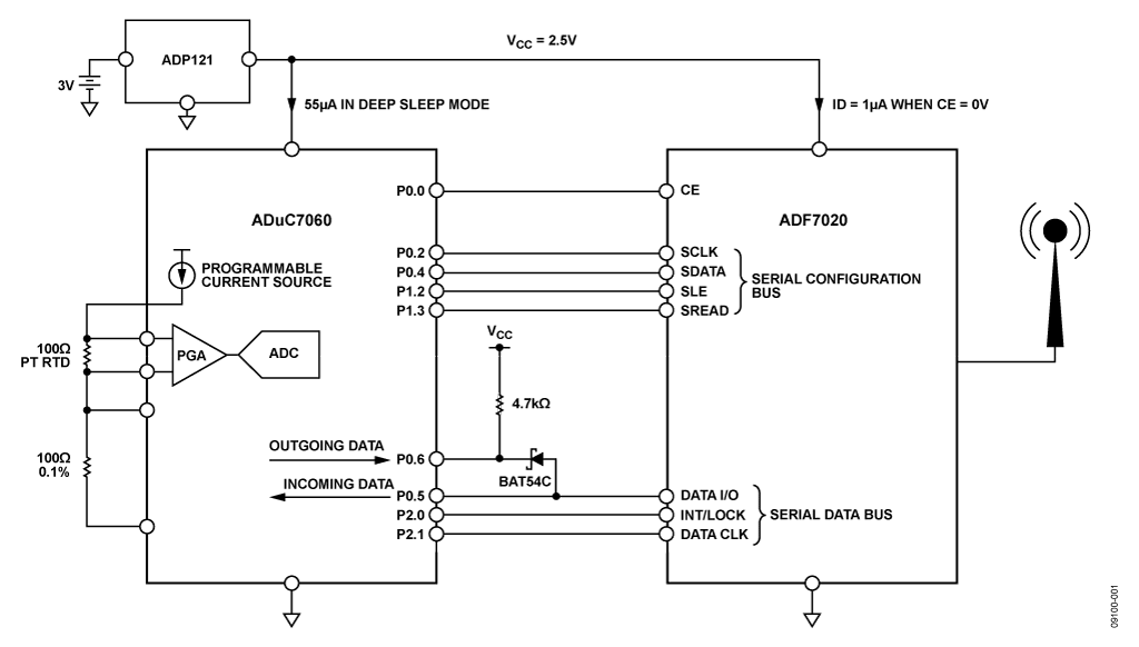
Connecting the ADF7020 ISM transceiver and the ADuC7060 precision microcontroller are two buses. Both are serial bidirectional buses: one bus is responsible for configuring the transceiver and requires four microprocessor ports; the other bus is a data bus used to transfer data between the controller and the transceiver, which requires at least three microprocessor port. In this application, two ports are used instead of a single bidirectional port with two interrupts. This simplifies the software, but requires the use of additional diodes and resistors to separate the input and output data streams. The parallel combination of two Schottky diodes ensures a logic low level below 200 mV. The BAT54C has two diodes in the same package (connect pin 1 and pin 2 to get a parallel configuration). All digital ports on the ADuC7060 have programmable pull-up resistors; however, external pull-up resistors are also required. For 10 kbps data rates, a 4.7 kΩ resistor works well.
The total current drawn by the circuit depends on three factors: the requirements of the individual components in sleep and active modes, the time the system is active, and the time the transceiver itself is active.
The first factor is addressed by selecting low-power components, such as the ADuC7060 and ADF7020. The second factor, minimizing system activity, is achieved by keeping the system inactive for as long as possible. A trade-off between integer and floating point arithmetic can be considered, in many cases integer is sufficient, its execution time is shorter and therefore more power efficient. The last factor, reduced transfer time, can be achieved in part by using a minimal-overhead protocol, but primarily by using the ADF7020, which has extremely high receiver sensitivity and excellent out-of-band rejection to maximize data containment. Probability of correct data.
Code Description - Overview
The system spends most of its time in deep sleep mode, consuming 50 μA to 60 μA (depending on ambient temperature). Timer 2 wakes the system up once every second. An ADC measurement is performed every 60 seconds, the results are linearized and sent. Timer 2 can wake the system from deep sleep; the other three timers do not have this function. Timer 2 is a 16-bit device, meaning it wakes up once per second (in sleep mode) when running on a 32 kHz clock. After starting the ADC, the system enters suspend mode (see ADuC7060 data sheet). This is also a low power mode, although not as low as deep sleep levels. After completion, the ADC wakes up the system. Calculate the temperature value based on the ADC results, package the data and send it.
Packing actually means placing the appropriate data in the buffer. The data at this time contains a 4-byte floating point temperature value and a 2-byte CRC (cyclic redundancy check). In more complex systems, this data is preceded by node address headers, received signal strength, and other information. Before sending this buffered data to the ADF7020 transceiver, an 8-byte preamble (used to help synchronize the receiving node) and a 3-byte synchronization word are sent. The latter is a unique 3-byte number that the receiving node checks for a match before receiving the packet.
The hardware on the receiving end is very similar; an ADF7020 transceiver is configured to receive a unique sync word at any time. The data packet is received after the synchronization word is received. Data is sent to PC via UART.
Shown in Figure 2 is the flow chart of the main loop of the measuring node and the basic receiving node.


Code description - ADF7020 driver
The ADF7020 supports multiple modulation schemes. In this example, GFSK (Gaussian Frequency Shift Keying) is used. The advantage of this solution is excellent spectral efficiency. In this mode, the ADF7020 generates data clocks both when transmitting and when receiving. The rising edge of the clock (DATA CLK) generates an interrupt, causing the ADuC7060 to place data bit by bit on the output port as shown in Figure 3. After all data is output, chip selection is released and the ADuC7060 re-enters deep sleep mode.
On the receiving side, the ADF7020 generates an interrupt (the INT/LOCK port remains high for nine clock cycles) after receiving a matching sync word.
This signal tells the ADuC7060 processor to prepare to receive data packets. Each bit received from the packet generates an interrupt within the ADuC7060. In the interrupt service routine (ISR), the bit stream is read and stored in the buffer. After all bytes within the packet have been received, a flag is set indicating that a new packet has been received. The main loop can now confirm the validity of the packet via checksum. Correct and complete packets are then processed. In this example, the above information is sent to the PC through UART for display. As shown in Figure 4, the same ISR can both receive data from and send data to the ADF7020 transceiver.


Blockdiagram
All reference designs on this site are sourced from major semiconductor manufacturers or collected online for learning and research. The copyright belongs to the semiconductor manufacturer or the original author. If you believe that the reference design of this site infringes upon your relevant rights and interests, please send us a rights notice. As a neutral platform service provider, we will take measures to delete the relevant content in accordance with relevant laws after receiving the relevant notice from the rights holder. Please send relevant notifications to email: bbs_service@eeworld.com.cn.
It is your responsibility to test the circuit yourself and determine its suitability for you. EEWorld will not be liable for direct, indirect, special, incidental, consequential or punitive damages arising from any cause or anything connected to any reference design used.
Supported by EEWorld Datasheet
EEWorld
subscription
account

EEWorld
service
account

Automotive
development
community

Robot
development
community

About Us Customer Service Contact Information Datasheet Sitemap LatestNews


Room 1530, 15th Floor, Building B,
No.18 Zhongguancun Street,
Haidian District,
Beijing, Postal Code: 100190
China
Telephone: 008610 8235 0740
 京公网安备 11010802033920号

 1200SGH2029F2HB


