The circuit shown in Figure 1 is a flexible signal conditioning circuit designed to handle signals with a wide dynamic range (from a few mV pp to 20 V pp). This circuit utilizes the internal programmable gain amplifier (PGA) of the high-resolution analog-to-digital converter (ADC) to provide the necessary conditioning and level translation and achieve dynamic range.
In process control and industrial automation applications, ±10 V full-scale signals are very common; however, in some cases the signal can be as small as a few mV. When processing ±10 V signals with modern low-voltage ADCs, attenuation and level conversion are necessary. However, for small signals, amplification is required to take advantage of the ADC's dynamic range. Therefore, when the input signal has a large variation range, a circuit with a programmable gain function needs to be used.
In addition, small signals may have larger common-mode voltage swings; thus requiring higher common-mode rejection (CMR) performance. In some applications with large source impedances, the analog front-end input circuitry also needs to be high impedance.


The circuit shown in Figure 1 solves all of these challenges and provides programmable gain, high CMR, and high input impedance. The input signal passes through a 4-channel ADG1409 multiplexer and enters the AD8226 low-cost, wide input range instrumentation amplifier. The AD8226 is a low-cost, wide-input-range instrumentation amplifier. The AD8226 provides high common-mode rejection (CMR) of up to 80dB and very high input impedance (800ΩM in differential mode and 400ΩM in common mode). The wide input range and rail-to-rail output allow the AD8226 to fully utilize the supply rails.
AD8475 is a fully differential attenuation amplifier that integrates precision gain resistors and can provide precision attenuation (G=0.4 or G=0.8), common-mode level conversion and single-ended differential conversion functions. The AD8475 is an easy-to-use, fully integrated precision gain block that handles signal levels up to ±10 V from a single supply. Therefore, the AD8475 is suitable for attenuating signals up to 20Vp-p from the AD8226 while maintaining high CMR performance and providing a differential output to drive a differential input ADC.
AD7192 is a 24-bit Σ-Δ ADC with built-in PGA. On-chip low-noise gain stages (G = 1, 8, 16, 32, 64, or 128) mean that small signals can be input directly to the ADC.
Combined with the above components, this circuit provides very good performance and is easy to configure for signals that vary in amplitude. This circuit is suitable for industrial automation, process control, instrumentation, and medical device applications.
The circuit contains an ADG1409 multiplexer, an AD8226 instrumentation amplifier, an AD8475 difference amplifier, an AD7192 Σ-Δ ADC (using an ADR444 reference), and the ADP1720 voltage regulator. Only a few external components are required to provide protection, filtering, and decoupling, making the circuit highly integrated and requiring less circuit board (printed circuit board [PCB]) area.
Regulator and Reference Selection
This circuit selects the ADP1720-5 as the 5 V regulator. It is a high voltage, micropower, low dropout linear regulator suitable for industrial applications.
This circuit selects the 4.096V ADR444 as the reference voltage source. It is an ultra-low noise, high-precision, low dropout device, especially suitable for high-resolution, Σ-Δ ADC and precision data acquisition systems.
Input switches and protection
The ADG1409 multiplexer has a 2-bit binary address line that can be used to select one of four possible input channels. The design also includes external protection features, such as standard diodes and transient voltage suppressors, to enhance the circuit's robustness. These are not shown in Figure 1, but are shown in the detailed schematics and other documentation of the CN0251 Design Support Package .
The ADG1409 multiplexer is configured to accept four differential input signals: (VS1A−VS1B), (VS2A−VS2B), (VS3A−VS3B), and (VS4A−VS4B). The outputs of the multiplexer (DA and DB) are applied to the input of the AD8226 instrumentation amplifier.
AD8226 input instrumentation amplifier
An external R G resistor sets the gain of the D8226. For this circuit, R G is omitted and the instrumentation amplifier stage has a gain of 1. Therefore, the output of the AD8226 is VSxA–VSxB, where x is the input channel number.
The differential input of the AD8226 is filtered by two 4.02k resistors and a 10nF capacitor, which form a single-pole RC filter with a cutoff frequency of 2.0kHz. Two 1nF capacitors add common-mode filtering with a cutoff frequency of 40kHz.
AD7192ADC PGA gain configuration
The AD7192 is configured to receive a differential analog input to match the differential output signal from the AD8475. The full-scale input range of the AD7192 is ±V REF /gain, where ±VREF = REFINx(+)-REFINx(-).
When the buffer in the AD7192 is enabled, the input channel drives the high-impedance input stage of the buffer amplifier. The absolute input voltage range in this mode is limited to AGND+250mV to AVDD-250mV. When the gain stage is enabled, the buffer output is applied to the input of the PGA, and the analog input range must be limited to ±(AV DD -1.25V)/gain because the PGA requires additional headroom. Therefore, when using a 4.096V reference voltage source and a 5V power supply, in order to make full use of the dynamic range of the ADC, the signal can be attenuated or amplified as shown in Table 1.
| Input range (VSxA − VSxB) |
AD8475 gain | AD7192 gain | PGA output range, bipolar mode (V) |
| ±10 V | 0.4 | 1 | ±4 |
| ±5 V | 0.8 | 1 | ±4 |
| ±1 V | 0.4 |
8 | ±3.2 |
| ±500mV | 0.8 | 8 | ±3.2 |
| ±250 mV | 0.8 | 16 |
±3.2 |
| ±125 mV | 0.8 | 32 |
±3.2 |
| ±62.5 mV | 0.8 | 64 | ±3.2 |
| ±31.25 mV | 0.8 | 128 | ±3.2 |
Differential Attenuation Amplifier
In order to drive a low-voltage ADC, the ±0V or ±5V signal needs to be attenuated and level shifted. If a differential amplifier configuration is used with precision resistors, CMR performance will degrade due to mismatch between the resistors. The AD8475 level shifter/attenuator integrates precision laser-trimmed matching resistors to ensure low gain error, low gain drift (33ppm/°C maximum), and high CMR characteristics.
The AD8475 offers two pin-selectable gain options, 0.4 and 0.8. The VOCM pin is used to adjust the output common-mode voltage for precision level translation to match the input range of the ADC and maximize dynamic range. This pin can be left floating and internally biased using a precision voltage divider consisting of two 200M resistors between supply and ground to provide the mid-supply voltage on this pin.
A single-pole differential RC filter consisting of two 100Ω resistors and a 1F capacitor acts as the anti-aliasing and noise reduction filter for the AD7192, with a cutoff frequency of 800Hz. Two 10nF capacitors provide common-mode filtering with a cutoff frequency of 160kHz.
Filter, output data rate and settling time
The AD7192 Σ-Δ ADC consists of a modulator and a digital filter. The output data rate (fADC) and settling time (tSETTLE) are related to the filter configuration and chopper configuration. Table 2 shows the output data rate and settling time calculations for different configurations.
| Chopping filter options | SINC3 | SINC4 |
| Disable | f ADC = f CLK /(1024 × FS[9:0]) t SETTLE = 3/f ADC
|
f ADC = f CLK /(1024 × FS[9:0]) t SETTLE = 4/f ADC
|
| Enable | f ADC = f CLK /(3 × 1024 × FS[9:0]) t SETTLE = 2/f ADC
|
f ADC = f CLK /(4 × 1024 × FS[9:0]) t SETTLE = 2/f ADC |
Layout considerations
The performance of this or any other high-speed/high-resolution circuit is highly dependent on proper PCB layout, including but not limited to power supply bypassing, signal routing, and proper power and ground planes. For details on PCB layout, see guides MT-031 and MT-101 and the article " A Practical Guide to High-Speed Printed Circuit Board Layout ."
System performance
The 24-bit AD7192 Σ-Δ ADC provides very good performance in this circuit. For more details on Σ-Δ ADCs, see tutorials MT-022 and MT-023 .
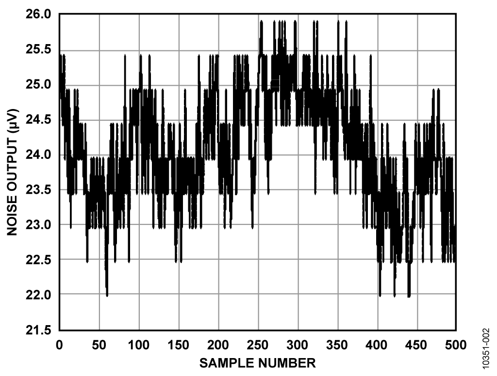
With the configuration set to chop disabled, an output data rate of 4.7 Hz, a gain of 1, and a SINC4 filter, the noise performance is shown in Figure 2 and the noise distribution histogram for 500 samples is shown in Figure 3 . The measured peak-to-peak noise in this circuit was approximately 3.9 μV (see Figure 2), and the rms noise was 860 nV. This equates to a peak-to-peak (noiseless code) resolution of 20 bits and an rms resolution of 23 bits. Table 3 shows the AD7192 rms noise for some data rates and gain settings with chopping disabled and a SINC4 filter used.


| filter word (decimal) | Output data rate (Hz) | Setup time (ms) | Gain 1 | Gain 8 | Gain 16 | Gain 32 | Gain 64 | Gain 128 |
| 1023 | 4.7 | 852.5 | 23.0 | 21.8 | 20.4 | 19.7 | 18.8 | 17.4 |
| 640 | 7.5 | 533 | 22.5 | 21.5 | 20 | 19.5 | 18.5 | 17.2 |
| 96 | 50 | 80 | 22.3 | 20.9 | 19.8 | 19.3 | 18.2 | 17 |
| 16 | 300 | 13.3 | 21.8 | 20.2 | 19.3 | 18.6 | 17.6 | 16.8 |
| 5 | 960 | 4.17 | 20.9 | 19.8 | 18.9 | 18 | 17.2 | 16.2 |
| 1 | 4800 | 0.83 | 19.2 | 19.0 | 18.4 |
17.6 | 16.6 | 15.8 |


Blockdiagram
All reference designs on this site are sourced from major semiconductor manufacturers or collected online for learning and research. The copyright belongs to the semiconductor manufacturer or the original author. If you believe that the reference design of this site infringes upon your relevant rights and interests, please send us a rights notice. As a neutral platform service provider, we will take measures to delete the relevant content in accordance with relevant laws after receiving the relevant notice from the rights holder. Please send relevant notifications to email: bbs_service@eeworld.com.cn.
It is your responsibility to test the circuit yourself and determine its suitability for you. EEWorld will not be liable for direct, indirect, special, incidental, consequential or punitive damages arising from any cause or anything connected to any reference design used.
Supported by EEWorld Datasheet
EEWorld
subscription
account

EEWorld
service
account

Automotive
development
community

Robot
development
community

About Us Customer Service Contact Information Datasheet Sitemap LatestNews


Room 1530, 15th Floor, Building B,
No.18 Zhongguancun Street,
Haidian District,
Beijing, Postal Code: 100190
China
Telephone: 008610 8235 0740
 京公网安备 11010802033920号

 1600HGG150112DB


