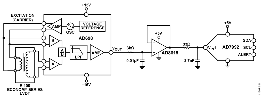
The circuit shown in Figure 1 is a complete adjustment-free linear variable differential transformer (LVDT) signal conditioning circuit. This circuit accurately measures linear displacement (position).
LVDTs are highly reliable sensors because their magnetic cores slide friction-free and have no contact with the inside of the tube. Therefore, LVDT is suitable for use in flight control feedback systems, position feedback in servo systems, automatic measurement in machine tools, and various other industrial and scientific research electromechanical applications that focus on long-term stability.
This circuit uses the AD698 LVDT signal conditioner, which contains a sine wave oscillator and a power amplifier to generate the excitation signal that drives the primary LVDT. The AD698 can also convert the secondary output to a DC voltage. The AD8615 rail-to-rail amplifier buffers the output of the AD698 and drives a low-power 12-bit successive approximation analog-to-digital converter (ADC). The system has a dynamic range of 82 dB and a bandwidth of 250 Hz, making it ideal for precision industrial positioning and metrology applications.
When powered by a ±15 V power supply, the system's signal conditioning circuit consumes only 15 mA; when powered by a +5 V power supply, the power consumption is 3 mA.
This circuit note discusses basic LVDT operating theory and design steps for optimizing the circuit in Figure 1 for a given bandwidth, including noise analysis and device selection considerations.

working principle
LVDTs are absolute displacement sensors that convert linear displacement or position from a mechanical reference point (or zero point) into a proportional electrical signal containing phase (direction) and amplitude (distance) information. No electrical contact is required between the moving parts (probe or core rod assembly) and the transformer to complete LVDT operation. It relies on electromagnetic coupling. For this reason, and because it operates without built-in electronic circuitry, LVDTs are widely used in applications where long life and high reliability are required in certain environments, such as military and aerospace applications.
For this circuit, Measurement Specialties™, Inc.'s E-100 economical LVDT sensor series is used in conjunction with the AD698. The E-Series has a linearity of ±0.5% over the entire range, making it suitable for most applications at moderate operating temperatures.
AD698 is a complete LVDT signal conditioning subsystem. It converts LVDT sensor mechanical position into unipolar DC voltage with high accuracy and repeatability. All circuit functions are integrated on-chip. By simply adding a few external passive components to set the frequency and gain, the AD698 can convert the raw LVDT secondary output into a proportional DC signal.
AD698 has a built-in low-distortion sine wave oscillator to drive the LVDT primary side. The sine wave frequency is determined by a single capacitor, with a frequency range of 20 Hz to 20 kHz and an amplitude range of 2 V RMS to 24 V RMS.
The LVDT secondary output consists of two sine waves and is used to directly drive the AD698. The AD698 decodes an LVDT by simultaneously demodulating the amplitude modulated input (secondary, A) and a fixed input reference voltage (primary, summed secondary, or fixed input, B). A common problem with previous solutions is that any drift in the amplitude of the driving oscillator leads directly to a gain error in the output. The AD698 calculates the ratio of the LVDT output to its input excitation, canceling out the effects of any drift, thus eliminating these errors. This device differs from the AD598 LVDT signal conditioner in that it has a different circuit transfer function and does not require the LVDT secondary summation (A + B) to be consistent with the stroke length.
The block diagram of AD698 is shown in Figure 2. The input consists of two independent simultaneous demodulation channels. The B channel monitors the LVDT drive excitation. C2 filters the full-wave rectified output and then sends it to the arithmetic circuit. Channel A performance is identical except that the comparator pin is provided externally. Since the A channel may reach a 0 V output when the LVDT is empty, the primary side voltage (B channel) is typically used to trigger the A channel's demodulator. Additionally, a phase compensation network may be required to add phase lead or lag to the A channel to compensate for the LVDT primary-to-secondary phase shift. For a half-bridge circuit, the phase shift is not important and the A-channel voltage is sufficient to trigger the demodulator.

After both channels have been demodulated and filtered, a voltage divider circuit equipped with a duty cycle multiplier is used to calculate the A/B ratio. The output of the voltage divider is the duty cycle. If A/B equals 1, the duty cycle is 100%. (This signal can be used if pulse width modulation output is required). The duty cycle driver circuit modulates and filters the reference current proportional to the duty cycle. The output amplifier regulates the 500 μA reference current and converts it to a voltage. The output transfer function is:

Device selection
Following the design procedure for dual-supply operation (±15 V) in the AD698 data sheet, set the excitation frequency to 2.5 kHz, the system bandwidth to 250 Hz, and the output voltage range to 0 V to 5 V.
The AD698's internal oscillator typically produces a small amount of ripple that is passed to the output. Use a passive low-pass filter to reduce this ripple to the required level.
There are certain trade-offs when choosing capacitor values to set the system bandwidth. Choosing a smaller capacitor value will give the system a higher bandwidth but will increase the output voltage ripple. This ripple can be suppressed by increasing the value of the parallel capacitance across the feedback resistor (which sets the output voltage level), but doing so increases the phase lag.
The AD8615 op amp buffers the output of the AD698, which ensures that the AD7992 ADC is driven from a low-impedance source (high-impedance sources will greatly reduce the AC performance of the ADC).
The low-pass filter is located between the output of the AD698 and the input of the AD8615 and serves two purposes:
The AD8615's internal protection circuitry allows the input to withstand input voltages higher than the supply voltage. This is important because the AD698's output voltage is capable of swinging ±11 V from ±15 V supplies. Higher voltages can be applied to the input as long as the input current is limited to 5 mA. This is mainly because the AD8615 (1 pA) has very low input bias current, allowing the use of larger resistors. Using these resistors increases thermal noise, causing the amplifier's overall output voltage noise to increase.
The AD8615 is an ideal amplifier for buffering and driving the input of the AD7992 12-bit SAR ADC because of its input overvoltage protection and the ability to swing rail-to-rail on both the input and output.
Noise analysis
If all signal conditioning components have been selected, the resolution required to convert the signal must be determined. As with most noise analyses, there are only a few key parameters to consider. Noise sources add up in RSS fashion; therefore, only consider any single noise source that is at least three to four times higher than other noise sources.
For LVDT signal conditioning circuits, the main source of output noise is the output ripple of the AD698. In comparison, the other noise sources (resistor noise, input voltage noise, and output voltage noise of the AD8615) are much smaller.
When the capacitor value is 0.39 μF and the parallel capacitance across the feedback resistor is 10 nF (as shown in Figure 3), the output voltage ripple of the AD698 is 0.4 mV rms. Note that the simplified schematic in Figure 1 does not show these devices and their associated pin connections; however, details can be found in the AD698 data sheet.


The maximum rms number that can be resolved can now be calculated by dividing the full-scale output by the total system rms noise.
![]()
The effective resolution is obtained by taking the logarithm of the total rms number, base 2.
![]()
Subtracting 2.7 bits from the effective resolution gives you the noise-free code resolution:

The total output dynamic range of a system can be calculated by dividing the full-scale output signal (5 V) by the total output rms noise (0.4 mV rms) and converting this to dB, which equals approximately 82 dB.
![]()
A good alternative device for this application is the AD7992, which has 12-bit resolution and a sampling rate of 188 kSPS per channel when used with a 3.4 MHz serial clock.
Phase lag/lead compensation
The AD698 multiplies the return signal with the input of the primary-side reference oscillator and demodulates it to produce an output signal. A small amount of phase shift will result in a large linear error, which is called undershoot on the output.
The phase lead network compensates for the −3° phase shift from primary to secondary in the E-100 Series LVDT. Figure 4 shows two different phase compensation networks.


When selecting component values for an appropriate network, it is important to note that RS and RT effectively form a resistive voltage divider, reducing the amplitude of the excitation signal before it reaches the ±ACOMP input of the AD698. This means that RT needs to be much larger than RS. The lag/lead circuit also places a load on the excitation output, so larger resistor values are recommended. The end goal is to achieve the desired phase lag/lead at the AD698 ACOMP input with a smaller amplitude drop.
The amount of phase lag/lead can be calculated according to the following equation:

Test Results
Using a Measurement Specialties, Inc. E-100 Economy LVDT connected to J3 and monitoring the output of the AD698 J6 on the EVAL-CN0301-SDPZ evaluation board with a digital oscilloscope, the actual output ripple is 6.6 mV pp, as shown in Figure 5.


The low-pass filter (3 kΩ, 0.01 μF) between the AD698 output and AD8615 input has a −3 dB bandwidth of 5.3 kHz and reduces ripple to 2 mV pp.
Since the low-pass filter is located between the AD698 output stage and the AD8615 input stage, data can be collected from the EVAL-CN0301-SDPZ evaluation board, as shown in Figure 6.
The AD698 's ripple is attenuated to 2 mV pp, and the system achieves 11 bits of noise-free code resolution.
For the complete design support package for this circuit note, see http://www.analog.com/CN0301-DesignSupport .
Applications in flight control surface position feedback
In the United States, unmanned aerial vehicles (UAVs), or drones, are playing an increasingly important role in national security. These high-tech, complex aerial work platforms are controlled by personnel miles away and support multiple missions. They contain functions such as aerial reconnaissance, combat weapons platforms, battlefield command and control surveillance or unmanned aerial refueling.
This complex system on the UAV uses countless electronic sensors for precise control and feedback. To control the UAV's altitude (pitch, roll, and yaw), actuators are used to apply force to the flight control surfaces. The ability of these actuators to accurately measure position is critical to maintaining the correct flight path.
Sensors used to measure actuator position need to meet three basic criteria: high accuracy, high reliability and light weight. The LVDT designed by Measurement Specialties, Inc. meets all three properties.
Multiple LVDTs working simultaneously
There are many applications where a large number of LVDTs are used in close proximity, such as multi-count measurements. If these LVDTs operate at similar carrier frequencies, stray magnetic coupling may cause beat frequencies. The resulting beat frequency may affect measurement accuracy under these conditions. To avoid this situation, all LVDTs work synchronously.
The EVAL-CN0301-SDPZ board can be configured to form a master oscillator between two LVDTs (using shorting jumpers to connect jumpers JP1, JP2, and JP4, and leaving JP3 unconnected). Each LVDT primary is driven with its own power amplifier to share the thermal load between AD698 devices.


Blockdiagram
All reference designs on this site are sourced from major semiconductor manufacturers or collected online for learning and research. The copyright belongs to the semiconductor manufacturer or the original author. If you believe that the reference design of this site infringes upon your relevant rights and interests, please send us a rights notice. As a neutral platform service provider, we will take measures to delete the relevant content in accordance with relevant laws after receiving the relevant notice from the rights holder. Please send relevant notifications to email: bbs_service@eeworld.com.cn.
It is your responsibility to test the circuit yourself and determine its suitability for you. EEWorld will not be liable for direct, indirect, special, incidental, consequential or punitive damages arising from any cause or anything connected to any reference design used.
Supported by EEWorld Datasheet
EEWorld
subscription
account

EEWorld
service
account

Automotive
development
community

Robot
development
community

About Us Customer Service Contact Information Datasheet Sitemap LatestNews


Room 1530, 15th Floor, Building B,
No.18 Zhongguancun Street,
Haidian District,
Beijing, Postal Code: 100190
China
Telephone: 008610 8235 0740
 京公网安备 11010802033920号


 RM242-050-211-5503


