As shown in Figure 1, this circuit highlights the easy interfacing of the ADF4350 wideband frequency synthesizer with integrated VCO to the ADL5380 and ADL5387 wideband I/Q demodulators. In this circuit, the ADF4350 provides a high-frequency, low-phase noise local oscillator (LO) signal for a wideband I/Q demodulator.
This circuit configuration has many advantages and is attractive for applications requiring quadrature mixing to baseband or intermediate frequencies.
The ADF4350 provides an RF differential output, and similarly, the ADL5380/ADL5387 accept differential inputs. This interface is easy to use and offers performance advantages. The differential signaling configuration reduces common-mode noise and eliminates even-order LO harmonics, thereby maintaining the quadrature accuracy of the I/Q demodulator. Additionally, the output power level of the ADF4350 closely matches the input power requirements of the quadrature demodulator, so no LO buffer is required.
The ADF4350 output covers a wide frequency range from 137.5 MHz to 4400 MHz. The ADL5387 frequency range is from 50 MHz to 2 GHz, while the ADL5380 covers the higher frequency range from 400 MHz to 6 GHz. Between the ADL5380 and ADL5387, the RF input range is from 50 MHz to 6 GHz. Therefore, the two-chip circuit configuration shown in Figure 1 can cover a wide frequency range from 50 MHz to 4400 GHz.


The ADF4350 is a wideband fractional-N and integer-N phase-locked loop frequency synthesizer covering the frequency range from 137.5 MHz to 4400 MHz. It features an integrated voltage-controlled oscillator (VCO) with a fundamental frequency range from 2200 MHz to 4400 MHz. The ADF4350 provides high-quality frequency synthesizer performance. However, depending on the demodulator architecture, LO filtering may be required to minimize the impact of PLL harmonics on the quadrature accuracy of the I/Q demodulator.
Analog Devices offers quadrature demodulators covering a wide frequency range. The ADL5387 frequency range is from 50 MHz to 2 GHz, while the ADL5380 covers the higher frequency range from 400 MHz to 6 GHz. The ADL5387 and ADL5380 utilize two different architectures to create a 90° phase shift between the I and Q paths. The ADL5387 utilizes a 2 × LO architecture where the local oscillator is twice the RF frequency, while the ADL5380 uses a polyphase filter-based phase splitter. Relative to 2 × LO-based phase splitters, polyphase architectures have narrower fractional bandwidths (i.e., operate in fewer octaves) and are more sensitive to PLL harmonics. Therefore, the ADL5380 requires harmonic filtering of the LO to maintain the quadrature accuracy of the I/Q demodulator, whereas the 2 × LO-based ADL5387 only requires filtering at the top end of its frequency range.


Figure 2 shows a simplified 2 × LO phase splitter implemented in the ADL5387. The 90° phase shift of the LO path is achieved through digital circuitry using D-type flip-flops and inverters. This architecture requires an external LO operating at twice the frequency of the required LO.


Figure 3 shows a simplified first-order polyphase circuit implemented in the ADL5380. This polyphase circuit contains complementary RC subcircuits to create a low-pass transfer function from the input to one output and a high-pass transfer function from the input to the other output. If the R and C values of the two polyphase paths match, then both paths have the same corner frequency and, more importantly, one output tracks the other with a 90° phase shift.
Interface between ADF4350 PLL and ADL5387 I/Q demodulator
The ADL5387 and ADL5380 I/Q demodulators utilize different architectures to achieve the ultimate goal of generating accurate quadrature signals. When interfacing with an LO frequency synthesizer such as the ADF4350, the way the architecture responds to the LO signal and harmonics must be considered. This will determine the LO filtering requirements. Figure 4 shows the basic interface between the ADF4350 and ADL5387. Depending on the operating frequency, an LO harmonic filter may be required between the ADF4350 and ADL5387.


In a 2 × LO based phase splitter, the quadrature accuracy depends on the duty cycle accuracy of the input LO.
The matching of the internal divider flip-flops also affects quadrature accuracy, but only slightly. It is important to have an externally applied LO with a 50% duty cycle to reduce quadrature errors. Additionally, any imbalance in rise and fall times will cause even-order harmonics to appear. When the demodulator LO input is driven differentially, even orders of harmonics can be eliminated, improving overall quadrature generation performance.
With a target image rejection of −40 dBc, Figure 5 shows the performance of the ADL5387 and ADF4350 with and without filtering for the differential LO source. The blue signal trace representing the "signal generator" is the ideal situation, where a Rhode & Schwarz signal generator is used to generate the LO with a sinusoidal output and harmonic levels much lower than the ADF4350. This is the ideal situation and the target comparison point. As can be seen from Figure 5, no filtering is required at frequencies below 1 GHz. However, above 1 GHz, small errors caused by LO harmonics account for a larger percentage of the input period. In this case, filtering should be used to further attenuate the even-order harmonics of the LO in order to achieve the specified quadrature accuracy of the I/Q demodulator.


Interface between ADF4350 PLL and ADL5380 quadrature demodulator
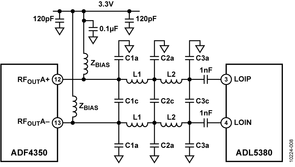
Unlike the ADL5387, the polyphase architecture of the ADL5380 phase splitter requires filtering of the ADF4350 output, as shown in Figure 6. The filtering is performed to attenuate the odd-order harmonics of the LO, thereby minimizing errors within the ADL5380 quadrature generation module. Measurement and simulation results in CN-0134 show that odd-order harmonics have a greater impact on quadrature errors than even-order harmonics. Figure 7 shows the measurement results when applying the ADF4350 output to the differential LO input of the ADL5380 after performing filtering. After filtering, the resulting image rejection is comparable to what is achievable with low-harmonic signal generators.


Filtering requirements
In summary, performing LO filtering on the ADF4350 output to suppress fundamental harmonics helps maintain the phase accuracy of the demodulator's quadrature signal. For the ADL5380 using a polyphase architecture, performing filtering is necessary. The ADL5387 architecture includes digital circuitry that is more resistant to LO signal harmonics. Therefore filtering can be omitted depending on the operating frequency.
Where filtering is required, Figure 8 shows an example LO output filter schematic and Table 1 lists the filter component values. This circuit is very flexible, offering four different filter options covering four different frequency bands. The filter is designed for 100 Ω differential input and 50 Ω differential output to match the LO input requirements of the demodulator and uses a Chebyshev response for optimal filter roll-off, but at the expense of increased channel ripple. For a more detailed discussion of ADF4350 output filtering, please refer to CN-0134.
| Frequency range (MHz) |
Z BIAS | L1 (nH) |
L2 (nH) |
C1a (pF) |
C1c (pF) |
C2a (pF) |
C2c (pF) |
C3a (pF) |
C3c (pF) |
| a. 500–1300 | 27nH|| 50Ω | 3.9 | 3.9 | DNI | 4.7 | DNI | 5.6 | DNI | 3.3 |
| b. 850–2450 | 19 nH || (100 Ω in C1c position) | 2.7 | 2.7 | 3.3 | 100Ω |
4.7 | DNI | 3.3 | DNI |
| c. 1250–2800 | 50Ω | 0Ω | 3.6 | DNI | DNI | 2.2 | DNI | 1.5 | DNI |
| d. 2800–4400 | 3.9nH | 0Ω | 0Ω | DNI | DNI | DNI | DNI | DNI | DNI |


Blockdiagram
All reference designs on this site are sourced from major semiconductor manufacturers or collected online for learning and research. The copyright belongs to the semiconductor manufacturer or the original author. If you believe that the reference design of this site infringes upon your relevant rights and interests, please send us a rights notice. As a neutral platform service provider, we will take measures to delete the relevant content in accordance with relevant laws after receiving the relevant notice from the rights holder. Please send relevant notifications to email: bbs_service@eeworld.com.cn.
It is your responsibility to test the circuit yourself and determine its suitability for you. EEWorld will not be liable for direct, indirect, special, incidental, consequential or punitive damages arising from any cause or anything connected to any reference design used.
Supported by EEWorld Datasheet
EEWorld
subscription
account

EEWorld
service
account

Automotive
development
community

Robot
development
community

About Us Customer Service Contact Information Datasheet Sitemap LatestNews


Room 1530, 15th Floor, Building B,
No.18 Zhongguancun Street,
Haidian District,
Beijing, Postal Code: 100190
China
Telephone: 008610 8235 0740
 京公网安备 11010802033920号

 XC6122E627ML


