The circuit shown in Figure 1 is a precision electronic scale signal conditioning system that uses a low-power buffered 24-bit Σ-Δ ADC AD7791 and two external zero-drift amplifiers ADA4528-1 . The solution operates from a single supply and provides high DC gain.
The front end uses an ultra-low noise, low offset voltage, low drift amplifier to amplify the low level signals from the load cell. For a load cell with a full-scale output of 10 mV, this circuit provides 15.3 bits of noise-free code resolution.
This circuit provides great flexibility in designing a custom low-level signal conditioning front-end, allowing users to easily optimize the overall transfer function of the sensor-amplifier-converter combination circuit. The AD7791 maintains good performance over the full output data rate range of 9.5 Hz to 120 Hz and can be used in a variety of scale applications operating at lower speeds.


Figure 2 shows the actual test setup. For testing, a 6-wire Tedea-Huntleigh 505H-0002-F070 load cell was used.
The current flowing through the PCB traces will produce an IR voltage drop. When the traces are long, this voltage drop may reach several millivolts or more, causing considerable errors. At room temperature, a 1-ounce copper trace that is 1 inch long and 0.005 inches wide has a resistance of about 100 mΩ. With a load current of 10 mA, this trace can cause an error of 1 mV.
In addition to the excitation, ground, and two output connections, the 6-wire load cell has two sense pins. These sense pins are connected to the high side (excitation pin) and the low side (ground pin) of the Wheatstone bridge respectively. Although there is a certain voltage drop across the line resistance, the voltage developed across the bridge can be accurately measured. In addition, the AD7791 accepts differential analog inputs and differential reference voltages. These two sense pins are connected to the AD7791 reference voltage input, forming a ratiometric configuration that is not affected by low-frequency changes in the power supply excitation voltage. Because of the ratiometric connection, a precision voltage reference is not required.
Unlike the 6-wire load cell, the 4-wire load cell does not have a detection pin, and the ADC differential reference voltage pin is directly connected to the excitation voltage and ground. With this connection, there is a voltage difference between the ADC's excitation pin and the reference voltage pin due to the line resistance. In addition, there will also be a voltage difference caused by line resistance on the low side (ground). This way the system will not be entirely ratiometric.
When the excitation voltage is 5 V, the Tedea-Huntleigh 2 kg load cell has a sensitivity of 2 mV/V and a full-scale output of 10 mV. Load cells also have an associated offset voltage or TARE. Additionally, load cells have gain errors. Some customers utilize DAC to eliminate or offset TARE. When the AD7791 uses a 5 V reference voltage, the differential analog input range is equal to ±5 V or 10 V pp. The circuit shown in Figure 1 amplifies the load cell output by a factor of 375 (1 + 2R1/RG), so the full-scale input range based on the load cell output is 10 V/375 = 27 mV pp. The AD7791's wide analog input range relative to the load cell's 10 mV pp full-scale signal helps ensure that the load cell's offset voltage and gain error do not overload the ADC front end.
The low-level amplitude signal from the load cell is amplified by two zero-drift amplifiers ADA4528-1. As the name suggests, a zero-drift amplifier has an offset voltage drift close to zero. The amplifier continuously corrects itself for any DC errors to remain as accurate as possible. In addition to low offset voltage and drift, zero-drift amplifiers are free of 1/f noise, an important feature that helps electronic scales make accurate measurements at DC or low frequencies.
Two op amps ADA4528-1 are configured as the first stage of a three op amp instrumentation amplifier. The third op amp is connected as a difference amplifier and is typically used in the second stage, but in the circuit shown in Figure 1, the differential inputs of the AD7791 perform this function.
The gain is equal to 1 + 2R1/RG. Capacitors C1 and C2 are placed in the feedback loop of the op amp and together with R1 and R2 form a low-pass filter with a 4.3 Hz cutoff frequency to limit the amount of noise entering the Σ-Δ ADC. C5, along with R3 and R4, forms a differential filter with a cutoff frequency of 8 Hz to further limit noise. C3 and C4 together with R3 and R4 form a common mode filter with a cutoff frequency of 159 Hz.
The ADP3301 low-noise regulator powers the AD7791, ADA4528-1, and load cells. In addition to the decoupling capacitors, noise reduction capacitors are provided at the regulator output as recommended in the ADP3301 data sheet. The regulator must be a low-noise type because any noise in the power supply or ground plane will cause noise in the system, causing circuit performance degradation.


The AD7791, a 24-bit Σ-Δ ADC, converts the amplified signal from the load cell. The AD7791 is configured for buffered operation to accommodate the impedance of the RC filter network on the analog input pins.
Figure 3 shows the rms noise of the AD7791 at different output data rates. This graph shows that the rms noise increases as the output data rate increases. However, the device maintains good noise performance over the entire output data rate range.


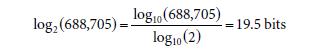
At a 9.5 Hz output data rate and a 2.5 V reference voltage, the AD7791 has an rms noise of 1.1 μV, resulting in a noise-free code number of
![]()
The coefficient 6.6 is used to convert the root mean square voltage to the peak to peak voltage.
Therefore, the corresponding noiseless code resolution is equal to:
Note that this is the performance of the AD7791 without a load cell or input amplifier connected.
The circuit shown in Figure 1 uses a 5 V reference voltage with a peak-to-peak input range of 10 V, so the LSB equals: It has a voltage noise density of 5.9 nV/√Hz. Therefore, the input amplifier and resistors add noise to the system. Additionally, the load cell itself can add noise.
The circuit shown in Figure 1 uses a 5 V reference voltage and a peak-to-peak input range of 10 V, so the LSB is equal to:
![]()
A 10 mV pp full-scale signal from the load cell produces a 3.75 V pp signal in the ADC, which is approximately 38% of the ADC range.
With the load cell connected (no load), obtain 7 sample sets, each containing 500 samples. The peak-to-peak code distribution is calculated for each sample set and then averaged to produce a code distribution of 159 sample points. Based on the ADC's 3.75 V pp full-scale input, this equates to 159 × 0.596 μV = 94.8 μV pp noise.
Therefore, the number of noise-free samples is equal to:
![]()
The corresponding noiseless code resolution of the overall system is equal to:
![]()
Figure 4 shows the ADC code plot for 500 samples (52.6 seconds, 9.5 Hz data rate). Note that the peak-to-peak distribution is approximately 160 codes.


Figure 5 shows the same data in histogram form. Figures 4 and 5 show the actual (raw) conversion results read back from the AD7791. In actual operation, electronic scale systems usually use digital post-filters. Performing additional averaging in the post-filter further increases the number of noise-free samples, but at a reduced data rate.
System resolution in grams is calculated as:

As with other high-precision circuits, proper layout, grounding, and decoupling techniques must be used. For more information, refer to Tutorial MT-031, "Grounding Data Converters and Solving the Mysteries of AGND and DGND ," and Tutorial MT-101, "Decoupling Techniques . " For the complete design support package for this circuit note, see www.analog.com/en/CN0216-DesignSupport .


Blockdiagram
All reference designs on this site are sourced from major semiconductor manufacturers or collected online for learning and research. The copyright belongs to the semiconductor manufacturer or the original author. If you believe that the reference design of this site infringes upon your relevant rights and interests, please send us a rights notice. As a neutral platform service provider, we will take measures to delete the relevant content in accordance with relevant laws after receiving the relevant notice from the rights holder. Please send relevant notifications to email: bbs_service@eeworld.com.cn.
It is your responsibility to test the circuit yourself and determine its suitability for you. EEWorld will not be liable for direct, indirect, special, incidental, consequential or punitive damages arising from any cause or anything connected to any reference design used.
Supported by EEWorld Datasheet
EEWorld
subscription
account

EEWorld
service
account

Automotive
development
community

Robot
development
community

About Us Customer Service Contact Information Datasheet Sitemap LatestNews


Room 1530, 15th Floor, Building B,
No.18 Zhongguancun Street,
Haidian District,
Beijing, Postal Code: 100190
China
Telephone: 008610 8235 0740
 京公网安备 11010802033920号

 VC14H15ET-2.000M


