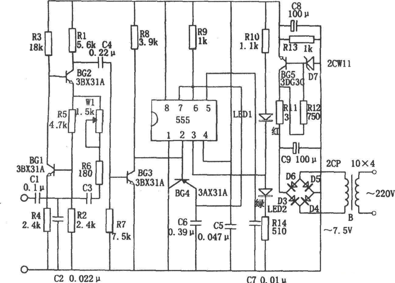
This reference design is an automotive-qualified isolated gate driver solution that drives silicon carbide (SiC) MOSFETs in a half-bridge configuration. This design provides two push-pull bias supplies for dual-channel isolated gate drivers, each providing +15V and –4V output voltages and 1W output power. The gate driver is capable of 4A peak source current and 6A peak sink current. The driver implements reinforced isolation and can withstand 8kV peak isolation voltage and 5.7kV RMS isolation voltage as well as common-mode transient immunity (CMTI) of over 100V/ns. This reference design includes a two-stage shutdown circuit that protects the MOSFET against voltage overshoot during short circuit conditions. DESAT detection threshold and second stage shutdown delay time are configurable. This design uses an ISO7721-Q1 digital isolator to connect the fault and reset signals. The overall design adopts a compact double-layer PCB board of 40mm × 40mm.


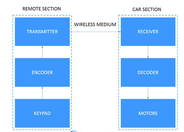
Blockdiagram
All reference designs on this site are sourced from major semiconductor manufacturers or collected online for learning and research. The copyright belongs to the semiconductor manufacturer or the original author. If you believe that the reference design of this site infringes upon your relevant rights and interests, please send us a rights notice. As a neutral platform service provider, we will take measures to delete the relevant content in accordance with relevant laws after receiving the relevant notice from the rights holder. Please send relevant notifications to email: bbs_service@eeworld.com.cn.
It is your responsibility to test the circuit yourself and determine its suitability for you. EEWorld will not be liable for direct, indirect, special, incidental, consequential or punitive damages arising from any cause or anything connected to any reference design used.
Supported by EEWorld Datasheet
EEWorld
subscription
account

EEWorld
service
account

Automotive
development
community

Robot
development
community

About Us Customer Service Contact Information Datasheet Sitemap LatestNews


Room 1530, 15th Floor, Building B,
No.18 Zhongguancun Street,
Haidian District,
Beijing, Postal Code: 100190
China
Telephone: 008610 8235 0740
 京公网安备 11010802033920号

 M38223E4-FS