* Based on GL3520 USB3.0 Hub hub design, one to four, with auxiliary power supply, 10 3CM PCB, with a shell, it is a small USB3.0 interface extender, using Type-C wire input, suitable for laptop peripherals and portable Equipment use, used to connect U disk, keyboard and mouse, etc. **
I would like to thank Lichuang EDA for conducting summer training camp activities and learning a lot of skills. The reason why I chose the USB3.0 Hub hub design topic based on GL3520 is, firstly, that I think this topic should be somewhat challenging; secondly, I happen to have the idea of a USB3.0 Hub. Without further ado, let’s get to the point. .
Current PCB version: V1.5, updated on 2020.8.5. Document version: V1.1, updated on 2020.8.19
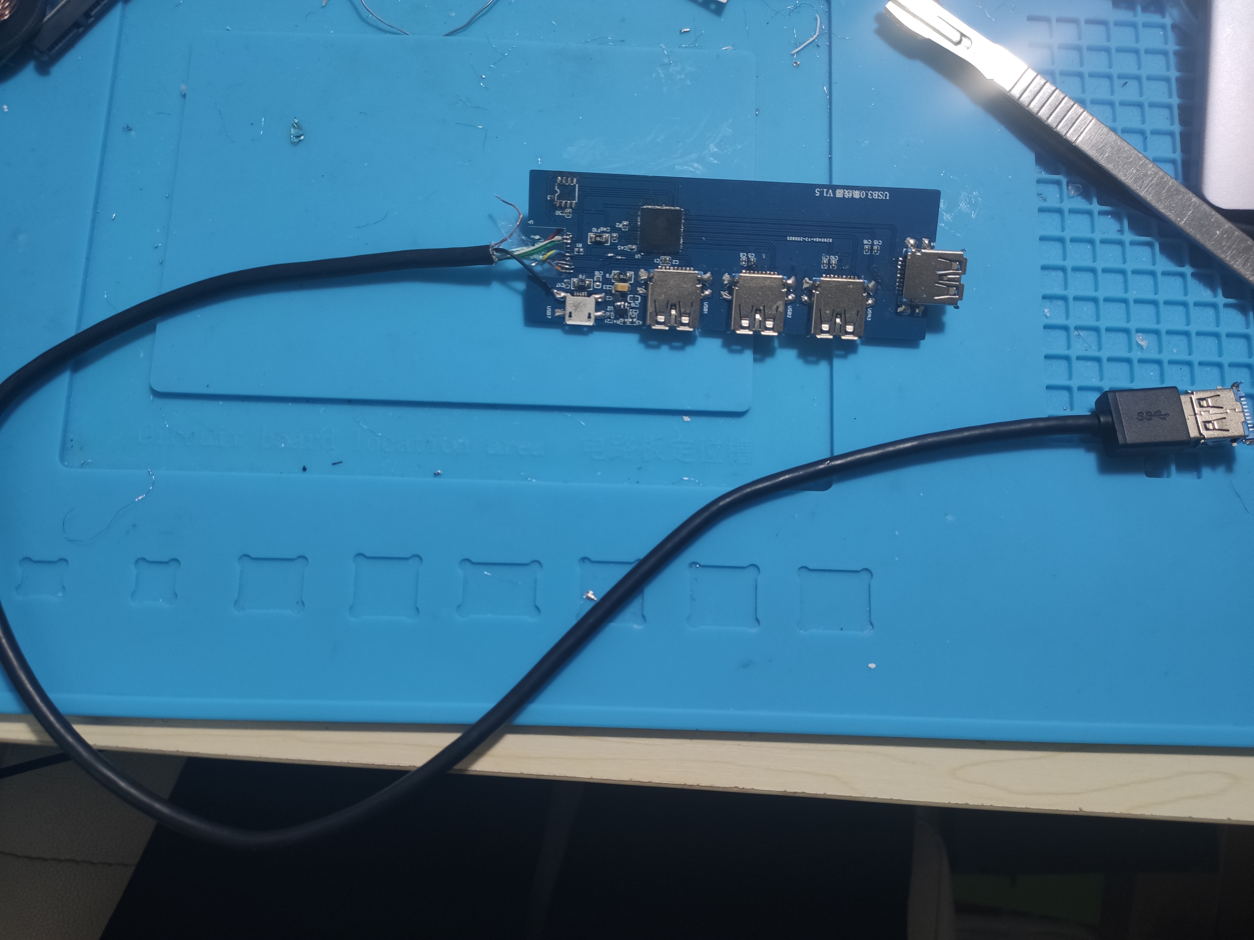
The picture was taken after welding was completed and was not cleaned. USB3.0-A cable and Type-c cable are used in a certain connection. After plugging it into the computer, 2.0 functions normally with a read and write speed of 30Mb/s. 3.0 can sometimes be recognized. Plug in the 3.0 U disk and enter 3.0 in the device manager. The device disappears.
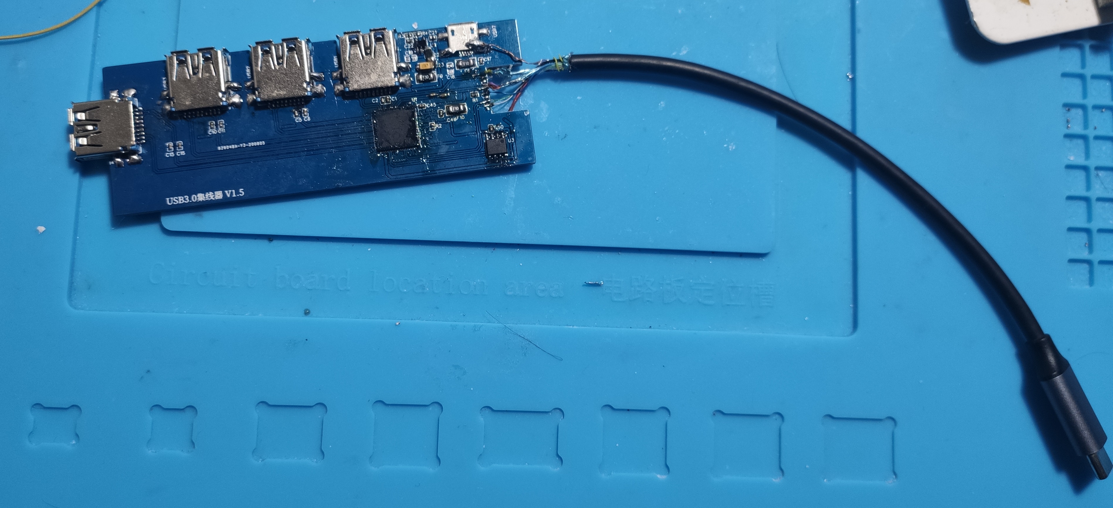
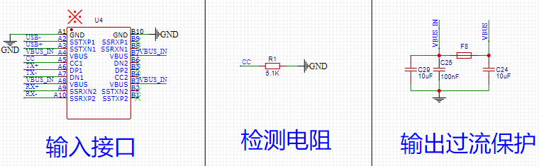
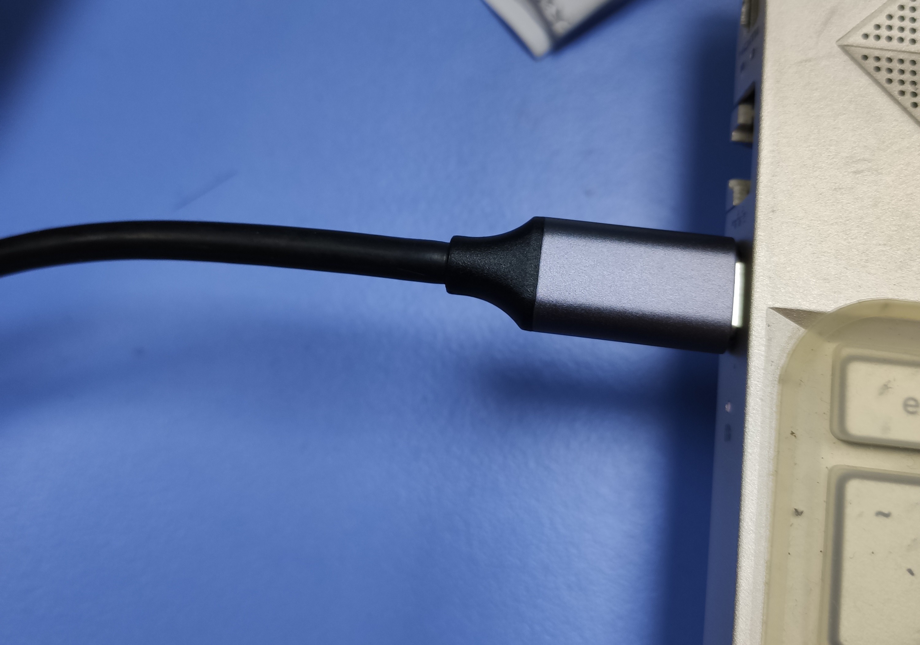
In the circuit design, considering space saving and practicality, the hub input (UFP) uses the Type-C interface, and the Type-C data cable is cut and welded on the PCB to lead to the input interface (here is a pit...); the hub output uses the sink Board-mounted USB3.0 interface, compatible with USB2.0.
Type-C interface is very common now, and it is necessary to understand some related contents: CC, DFP, UFP, DRP.
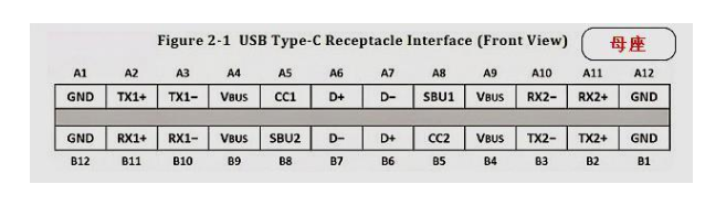
Configuration Channel, channel configuration pin. This is the key channel for Type-C. Its functions include detecting forward and reverse plugging, detecting USB connection identification, providing how much voltage and current, establishing and managing the connection between data and VBUS between USB devices, etc. The difference between universal fast charging cables and ordinary data cables (dual Type-C interfaces) on the market lies in the CC pin.
Downstream Facing Port can be understood as Host, and DFP provides VBUS and data. In the protocol specification, DFP specifically refers to the downstream transmission of data. In a general sense, it refers to the equipment for data downstream and external power supply. A typical DFP device is a power adapter.
Upstream Facing Port can be understood as Device. UFP takes power from VBUS and provides data. Typical UFP devices are USB flash drives and mobile hard drives.
Dual Role Port, a dual role port, can be used as either DFP (Host) or UFP (Device), and can also be dynamically switched between DFP and UFP. A typical DRP device is a laptop.
The input port of the hub uses a Type-C interface (UFP), which is directly connected to the Type-C port (DFP) of a computer or mobile device. The Type-C interface of the hub input end in the circuit is a UFP, and the CC pin is connected in series with a 5.1K resistor to the ground. Here is to set the input power, that is, to obtain VBUS. The input is overcurrent protected with a 6V/1A resettable fuse, and 10u and 0.1u filter out low-frequency and high-frequency clutter.
As shown below: Generally in Type-C, there are two CCs (CC1, CC2) on the DFP end, both of which are connected with pull-up resistors Rp, to detect UFP insertion and turn on/off VBUS. When that CC detects input, use That group of RX/TX; UFP terminal has only one CC, which needs to be connected to a pull-down resistor Rd to determine the DFP output power. If the CC pin on the UFP side is left floating, the DFP may not turn on the VBUS power output.
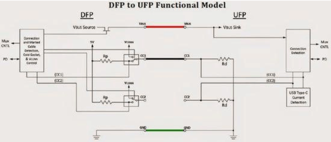
The value of Rd determines the DFP output power. The resistance range is not arbitrary and is defined by the Type-C interface standard protocol. Different interfaces and application scenarios have different values. Common resistance value selections and corresponding power supply capabilities:
Rd = 56k, using the default USB power supply capability;
Rd = 22k, using 5V/1A power supply capability;
Rd = 10k, using 5V3A power supply capability.
In this design, Rd chooses 5.1K. Why choose 5.1L here? This means that the output power is determined by the Rp of the DFP. If the resistance of Rp is different, the voltage detected by CC will be different, and then the DFP will be controlled to perform the corresponding power supply capability.
The output end of the hub uses 4 sinker-mounted USB3.0 type A interfaces, which are compatible with USB2.0 and can be connected to common USB devices. In the circuit, each output port is protected by a 6V/1A self-recovery fuse, and 10u and 0.1u filter out low-frequency and high-frequency noise.
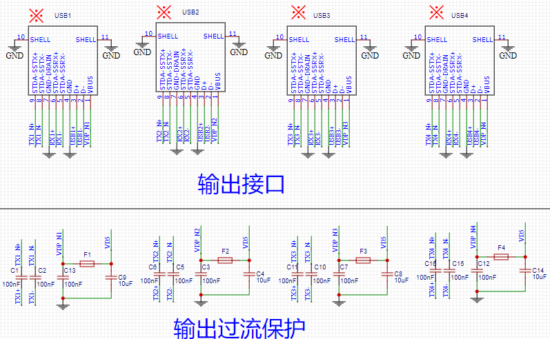
0.1u coupling capacitors are connected in series on the TX+ and TX- lines to separate the DC path between the port and the main control signal.
The main control is GL3520 according to the requirements of the topic. This design uses a PQFN-88 packaged chip, which has similar pins to the PQFN-64 package. PQFN-88 is mainly selected to facilitate later upgrades. The GL3520 main control has several special pins that require special attention during design, and are also described in the DataSheet. In the QFN88 package, the following pins are particularly important:
Pin3: RTERM, string 680 resistor to ground;
Pin74: PGANG, mode setting (100K pull-up: multi-group mode; 100K pull-down: single group);
Pin76: TEST, test (pull-up: enter test mode; ground: normal mode);
Pin78: OVCUR1J, short circuit protection (it needs to be pulled up to 3.3V if the short circuit protection function is not used);
Pin82: PSELF, power supply selection (pull-up: independent power supply; pull-down: bus power supply);
Pin83: RESETJ, reset (active low level, ≥40us);
These pins and related mode settings are detailed in the DataSheet, just check the DataSheet.
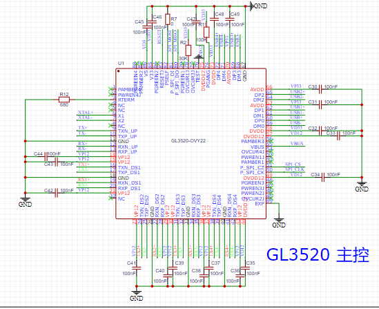
The main control is set to normal multi-group mode and uses bus power by default. The reset circuit uses a resistor-capacitor reset circuit and connects an external Flash chip. Regarding Flash, according to the DataSheet description, Flash is required for some special port configurations. There is no relevant explanation for the specific configuration. Flash can be omitted in the GL35xx USB2.0 design, and can also be removed in the general USB3.0 design (provided there is firmware in the chip).
GL3520 requires three levels of voltage: 1.2V, 3.3V, 5.0V.
1.2V is provided by an external LDO chip, with a maximum output of 1A.
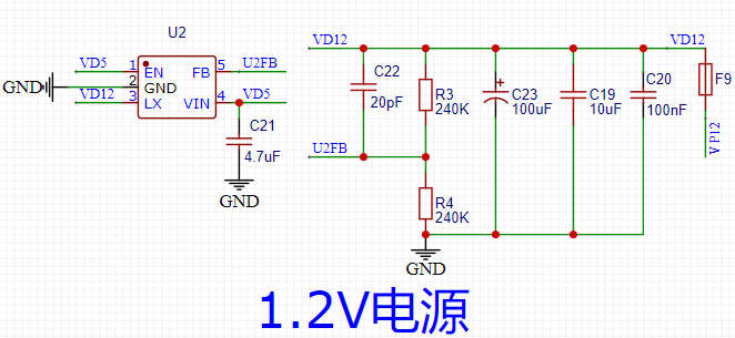
The 3.3V power supply uses the main control internal LDO output.
5.0V is provided by the input port VBUS.
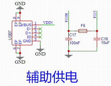
The auxiliary power supply does not have much design and is directly provided by external Micro USB. In fact, for general applications (connecting U disk, mouse, etc.) the auxiliary power supply can be omitted;
2020.8.5: The first version of PCB proofing, version number V1.5.
2020.8.11: PCB and components arrive.
2020.8.11 Night: Manual soldering, USB port and 1.2V power supply soldering completed, test passed.
2020.8.14: The welding of the circuit main control chip is completed. Plug in the computer,
Can recognize USB2.0 and USB3.0.
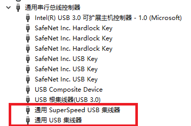
The hub can be recognized in the computer device management, but after plugging in the 3.0 U disk, the system pops up a message that the USB device is not working properly. After that, only 2.0 can be recognized in the device management; after unplugging the hub and plugging it in again, only 2.0 can still be recognized. When plugging in a 3.0 U disk, there is no response; when plugging in a 2.0 U disk, it works normally.
After writing the Flash to update the firmware, only 2.0 can be recognized.
Changing the input cable to a USB3.0-A interface still only recognizes 2.0.
After consulting relevant information, I found that the problem should lie in impedance matching (85~90ohm) and special pin configuration. Since Type-C jumpers are used in this design, there will be big problems with impedance matching (measured, solder joint size, solder tin Different shapes and lead lengths will affect 3.0 recognition); in addition, in the general design of GL3520, if you do not exchange RX-/+, TX-/+ and use special pin functions, you do not need to plug in Flash (provided there is firmware inside the chip) ).
V1.0: The submitted version of the assessment questions was sent to Jialichuang for PCB proofing, and the via diameter exceeded the manufacturing process.
V1.5: 2020.8.5 update:
1. Modify the diameter and position of the via;
2. Fine-tune the layout;
There is a problem:
1. The USB3.0 interface package size (drawn by myself) is different from the device;
2. Some silk screen printing positions on sides A and B are incorrect;
3. Only USB2.0 can be recognized.

All reference designs on this site are sourced from major semiconductor manufacturers or collected online for learning and research. The copyright belongs to the semiconductor manufacturer or the original author. If you believe that the reference design of this site infringes upon your relevant rights and interests, please send us a rights notice. As a neutral platform service provider, we will take measures to delete the relevant content in accordance with relevant laws after receiving the relevant notice from the rights holder. Please send relevant notifications to email: bbs_service@eeworld.com.cn.
It is your responsibility to test the circuit yourself and determine its suitability for you. EEWorld will not be liable for direct, indirect, special, incidental, consequential or punitive damages arising from any cause or anything connected to any reference design used.
Supported by EEWorld Datasheet
EEWorld
subscription
account

EEWorld
service
account

Automotive
development
community

Robot
development
community

About Us Customer Service Contact Information Datasheet Sitemap LatestNews


Room 1530, 15th Floor, Building B,
No.18 Zhongguancun Street,
Haidian District,
Beijing, Postal Code: 100190
China
Telephone: 008610 8235 0740
 京公网安备 11010802033920号

 154-000-003L999